Method for cancellation of the effect of charge feedthrough on CMOS pixel output

Active Publication Date: 2007-07-10
SMAL CAMERA TECH
View PDF4 Cites 35 Cited by
  • Summary
  • Abstract
  • Description
  • Claims
  • Application Information

AI Technical Summary

Benefits of technology

[0010]Therefore, it is desirable to provide a non-complex process for compensating for both CMOS fixed pattern noise and electronic charge feedthrough across CMOS pixel transistors. Furthermore, it is

Problems solved by technology

CMOS fixed-pattern noise is generally due to mismatches in the threshold voltages of the MOS transistors of a CMOS pixel, as well as being due to feedthrough of electronic charge, associated with the MOS pixel transistors, to the output of a pixel.
The dark offset reduces the available voltage swing of pixels, thereby limiting the dynamic range of the imager.
This double-sampling technique suffers, however, in that it does not enable the determination and/or correction of feedthrough of electronic charge across the pixel MOS transistors to the pixel output.
Moreover, due to the calibration factor application's complexity, the calibration factor application is typically enabled o

Method used


Image

  • Method for cancellation of the effect of charge feedthrough on CMOS pixel output
  • Method for cancellation of the effect of charge feedthrough on CMOS pixel output
  • Method for cancellation of the effect of charge feedthrough on CMOS pixel output

Examples


Embodiment Construction

[0026]The present invention will be described in connection with preferred embodiments; however, it will be understood that there is no intent to limit the present invention to the embodiments described herein. On the contrary, the intent is to cover all alternatives, modifications, and equivalents as may be included within the spirit and scope of the present invention as defined by the appended claims.

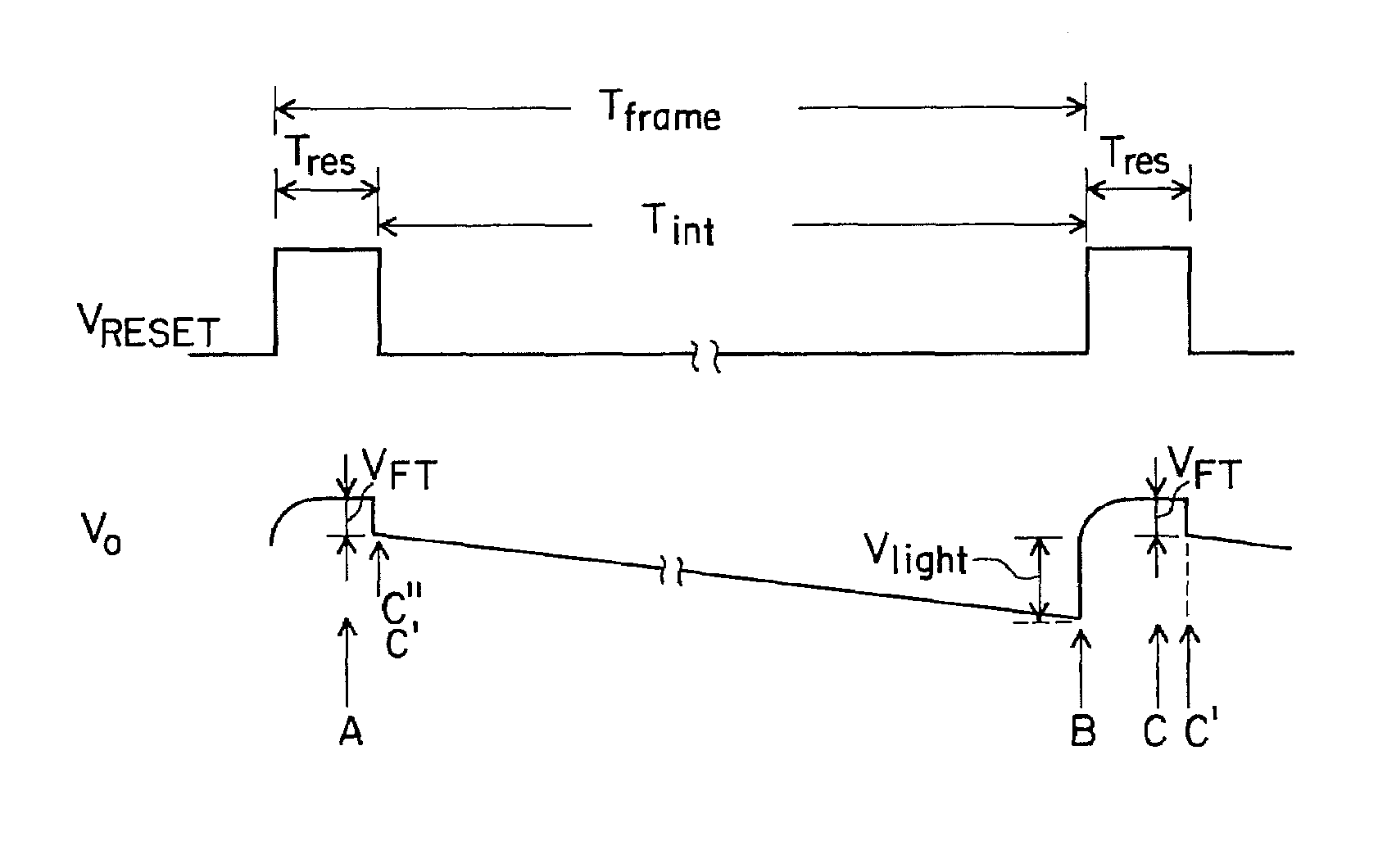
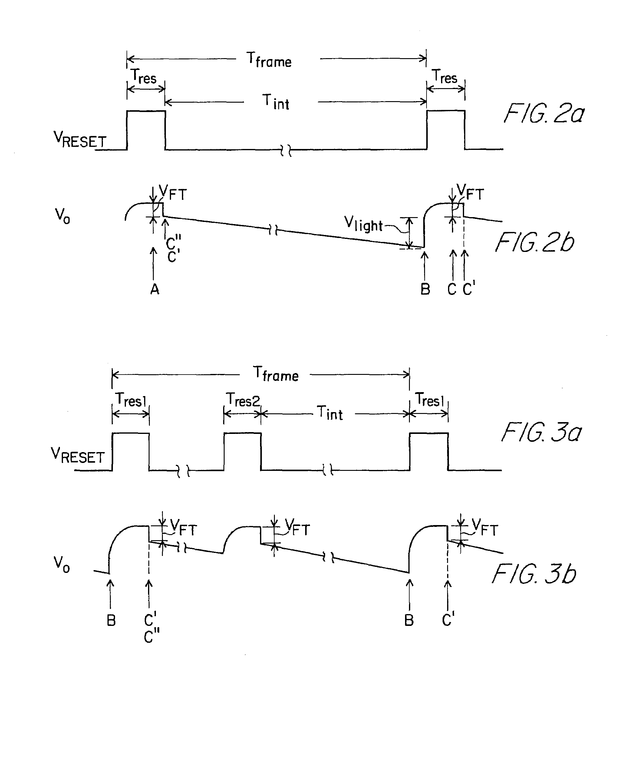
[0027]For a general understanding of the present invention, reference is made to the drawings. In the drawings, like reference have been used throughout to designate identical or equivalent elements. It is also noted that the various drawings illustrating the present invention are not drawn to scale and that certain regions have been purposely drawn disproportionately so that the features and concepts of the present invention could be properly illustrated.

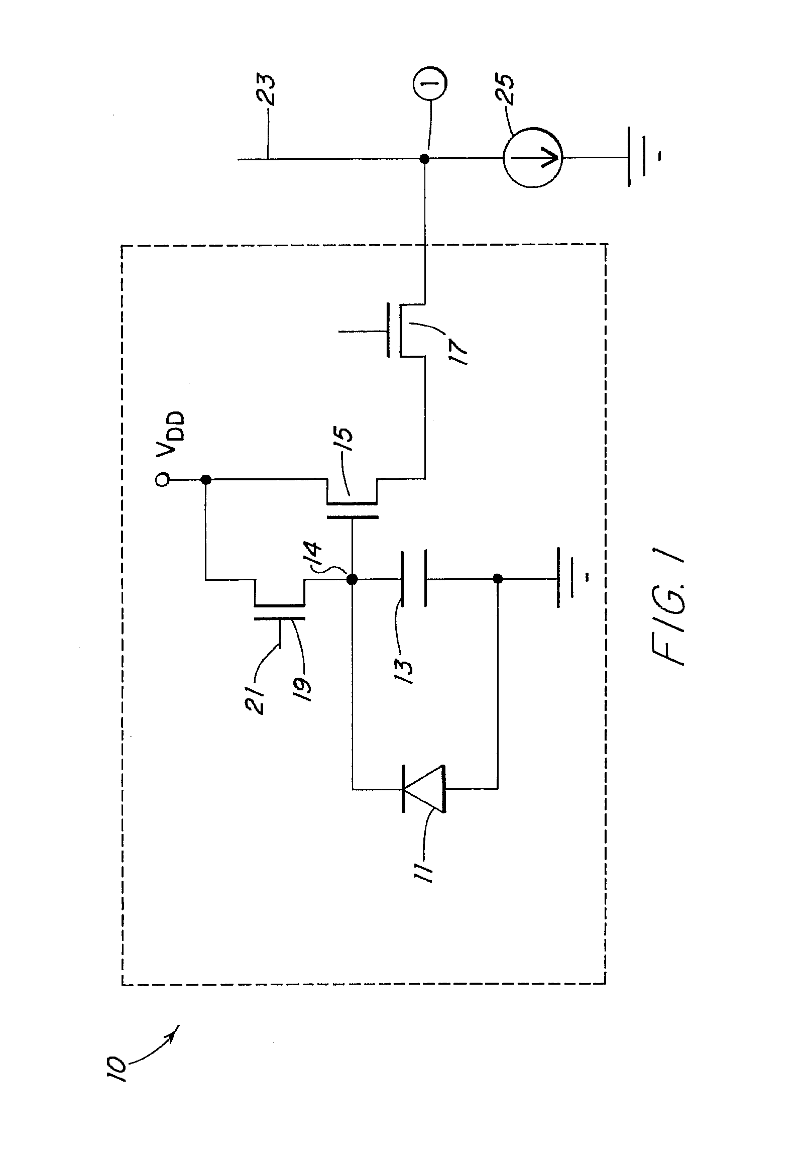
[0028]It is noted that in the descriptions below the references to a row select switch are not limited to a row select switch, but ...


PUM


Abstract

A method for determining a pixel output value of an imager; the imager having a plurality of pixels, a reset switch associated with each pixel and a select switch associated with each pixel; due to incident illumination upon a pixel of the imager after a reset period. The method captures a first pixel output value when the reset switch is OFF during a reset period and the select switch is ON during a reset period and captures a second pixel output value when the select switch is ON near an end of an integration period. If the second pixel output value is captured when the select switch is ON near an end of a first integration period, the first pixel output value may be captured when the reset switch is OFF during a reset period preceding the first integration period and the select switch is ON during a reset period preceding the first integration period. Moreover, if the second pixel output value is captured when the select switch is ON near an end of a first integration period, the first pixel output value may be captured when the reset switch is OFF during a reset period immediately following the first integration period and the select switch is ON during a reset period immediately following the first integration period.

Description

PRIORITY INFORMATION[0001]This application claims priority, under 35 U.S.C. § 119, from U.S. Provisional Patent Application Ser. No. 60 / 345,780, filed on Jan. 3, 2002; the entire contents of which are hereby incorporated by reference.FIELD OF THE PRESENT INVENTION[0002]The present invention relates to the determination of a pixel output voltage due to incident illumination upon a pixel of a CMOS digital imager during an integration period. More specifically, the present invention relates to the determination of a pixel output voltage due to incident illumination upon a pixel of a CMOS digital imager during an integration period which corrects for voltage feedthrough caused by a reset switch and / or select switch.BACKGROUND OF THE PRESENT INVENTION[0003]CMOS image sensors are attractive for use in a wide range of applications, such as still photography and video imaging products, due to their compatibility with VLSI circuit design and fabrication processing. Since low-cost, large-scal...

Claims


Application Information

Patent Timeline
IPC IPC(8): H04N3/14H04N5/335H04N5/351H04N5/365H04N5/374
CPCH04N5/3575H04N5/361H04N5/3745H04N25/616H04N25/63H04N25/77
Inventor LEE, HAE-SEUNGFIFE, KEITH GLEN
Owner SMAL CAMERA TECH
Why Eureka
Try Eureka