Reversed T-shaped FinFET

a technology of finfets and fins, applied in the field of transistors, can solve the problems of short channel effects, excessive leakage between the source and drain, and the limitation of conventional methods, and achieve the effect of short channel control and improved current drivability

Active Publication Date: 2007-07-31
GLOBALFOUNDRIES US INC
View PDF4 Cites 77 Cited by
  • Summary
  • Abstract
  • Description
  • Claims
  • Application Information

AI Technical Summary

Benefits of technology

[0005]Implementations consistent with the present invention provide a reversed T-shaped FinFET. The exemplary FinFET includes a fin formed in a reversed T-shape and a dielectric layer formed over surfaces of the fin to conform with the shape of the fin...

Problems solved by technology

The reduction of design features below 100 nm challenges the limitations of conventional methodology.
For example, when the gate length of conventional planar metal oxide semiconductor field effect transistors (MOSFETs) is scaled below 100 nm, problems associated with short ...

Method used


Image

  • Reversed T-shaped FinFET
  • Reversed T-shaped FinFET
  • Reversed T-shaped FinFET

Examples


Embodiment Construction

[0027]The following detailed description of the invention refers to the accompanying drawings. The same reference numbers in different drawings may identify the same or similar elements. Also, the following detailed description does not limit the invention. Instead, the scope of the invention is defined by the appended claims and their equivalents.

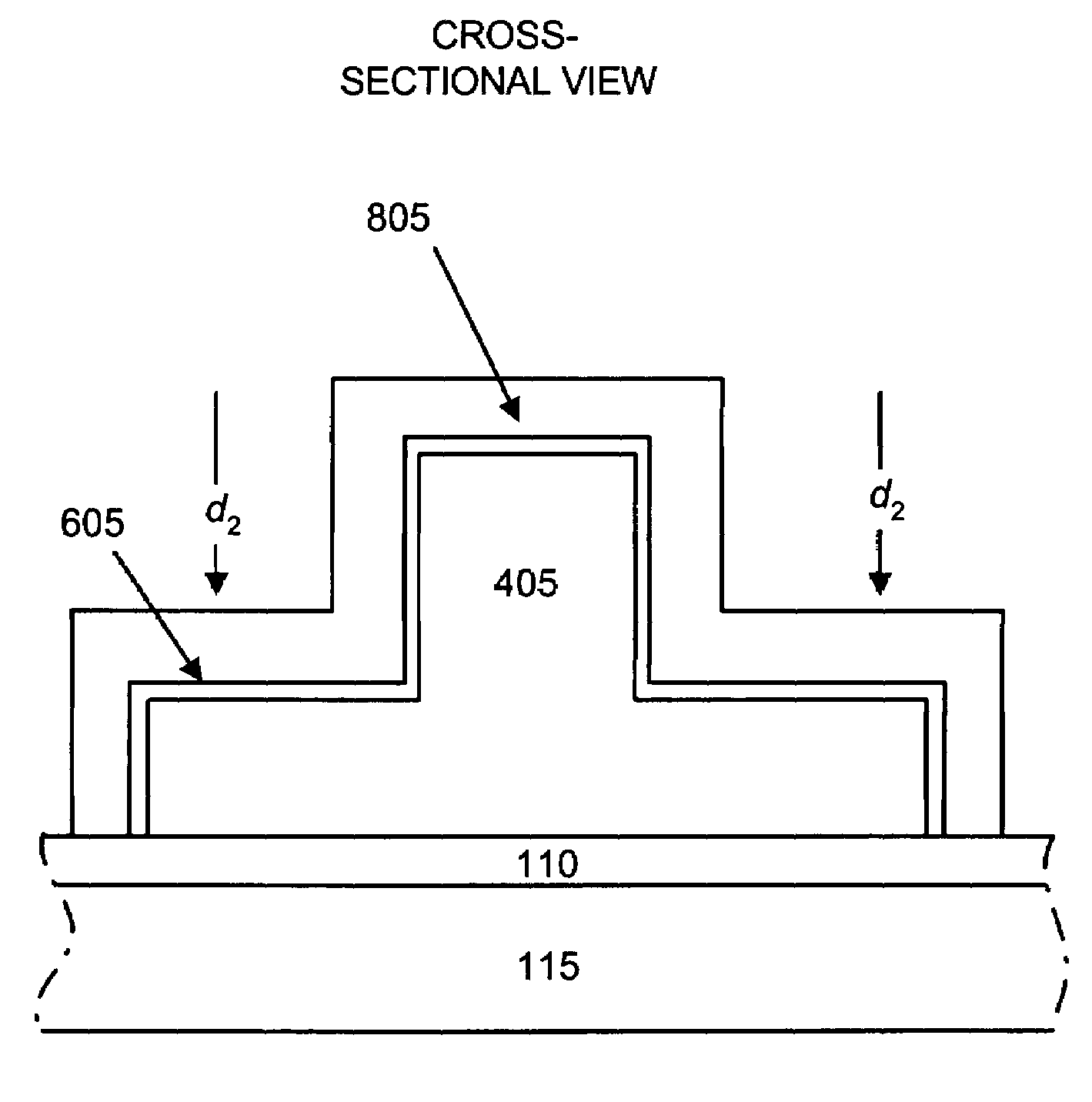
[0028]Consistent with the present invention, an exemplary reversed T-shaped FinFET is provided that achieves better current drivability and short channel control than conventional shaped FinFETs.

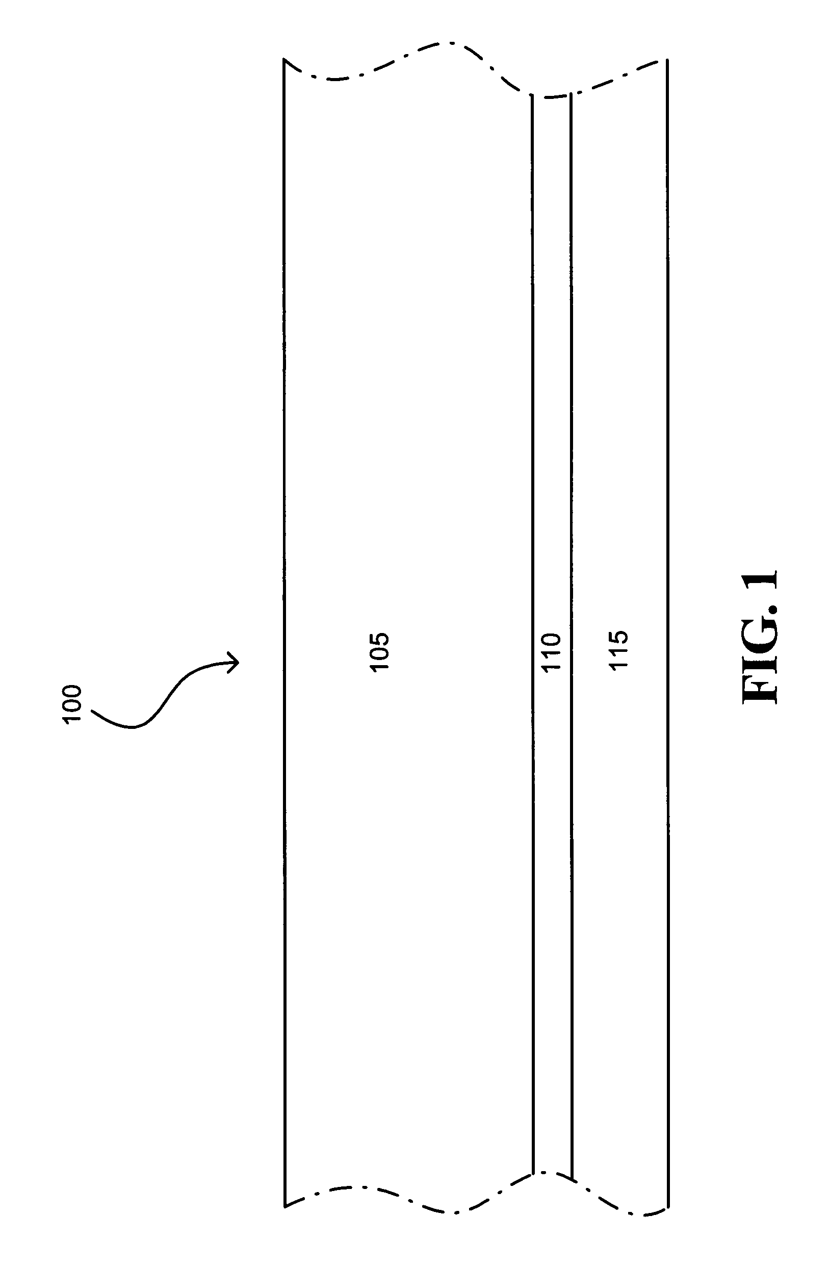
[0029]FIG. 1 illustrates a cross-section of a silicon on insulator (SOI) wafer 100 formed in accordance with an exemplary embodiment of the present invention. SOI wafer 100, consistent with the present invention, may include a buried oxide layer 110 formed on a substrate 115. A fin layer 105 may further be formed on buried oxide layer 110. The thickness of fin layer 105 may range, for example, from about 200 Å to about 1500 Å and the thickness of b...


PUM


Abstract

A fin field effect transistor (FinFET) includes a reversed T-shaped fin. The FinFET further includes source and drain regions formed adjacent the reversed T-shaped fin. The FinFET further includes a dielectric layer formed adjacent surfaces of the fin and a gate formed adjacent the dielectric layer.

Description

TECHNICAL FIELD[0001]The present invention relates generally to transistors and, more particularly, to fin field effect transistors (FinFETs).BACKGROUND ART[0002]The escalating demands for high density and performance associated with ultra large scale integration semiconductor devices require design features, such as gate lengths, below 100 nanometers (nm), high reliability and increased manufacturing throughput. The reduction of design features below 100 nm challenges the limitations of conventional methodology.[0003]For example, when the gate length of conventional planar metal oxide semiconductor field effect transistors (MOSFETs) is scaled below 100 nm, problems associated with short channel effects, such as excessive leakage between the source and drain, become increasingly difficult to overcome. In addition, mobility degradation and a number of process issues also make it difficult to scale conventional MOSFETs to include increasingly smaller device features. New device struct...

Claims


Application Information

Patent Timeline
IPC IPC(8): H01L29/76H01L27/08
CPCH01L29/42392H01L29/66795H01L29/7842H01L29/785
Inventor WANG, HAIHONGAHMED, SHIBLY S.LIN, MING-RENYU, BIN
Owner GLOBALFOUNDRIES US INC
Why Eureka
Try Eureka