Memory interface with write buffer and encoder
a memory interface and encoder technology, applied in the field of memory interfaces with write buffers and encoders, can solve the problems of negative affecting the performance of the memory, increasing the memory soft error rate, and more susceptible to the effects of cosmic radiation
- Summary
- Abstract
- Description
- Claims
- Application Information
AI Technical Summary
Problems solved by technology
Method used
Image

Examples
Embodiment Construction
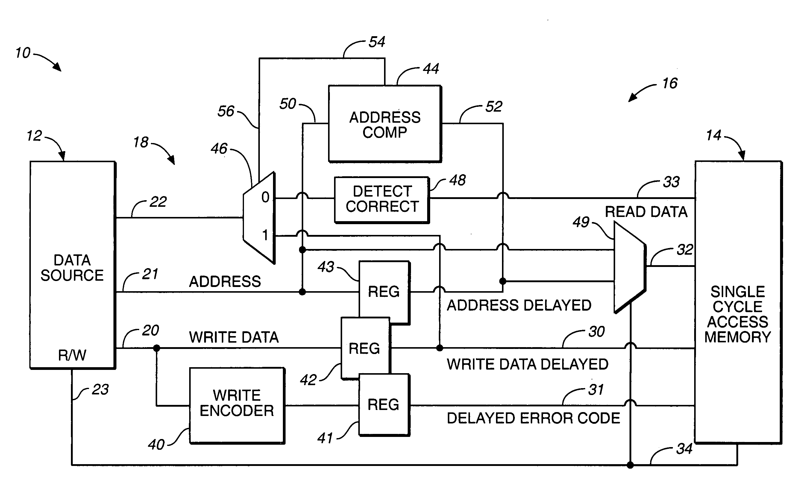
[0018]FIG. 1 is a block diagram illustrating a data storage and retrieval circuit 10 having error code generation circuitry, which does not adversely effect critical memory timing paths, according to one embodiment of the present invention. Circuit 10 supports full word write operations. An example of a circuit that supports full and partial word write operations is shown in FIG. 2. Referring to FIG. 1, circuit 10 includes a data source 12, a single cycle access memory 14 and a memory interface 16. In one embodiment, data source 12, memory 14 and memory interface 16 are embedded within a single semiconductor integrated circuit. However, these elements can be implemented on separate devices in alternative embodiments of the present invention.
[0019]Data source 12 can include any suitable data source, such as an embedded processor. Data source 12 includes an interface 18 having a write data output 20, a memory address output 21, a read data input 22, and a read / write control output 23....
PUM
 Abstract
Description
Claims
Application Information
 - R&D Engineer
- R&D Manager
- IP Professional
- Industry Leading Data Capabilities
- Powerful AI technology
- Patent DNA Extraction
Browse by: Latest US Patents, China's latest patents, Technical Efficacy Thesaurus, Application Domain, Technology Topic.
© 2024 PatSnap. All rights reserved.Legal|Privacy policy|Modern Slavery Act Transparency Statement|Sitemap