
Liquid crystal display device with light absorbing layers

a liquid crystal display and light absorbing layer technology, applied in semiconductor devices, identification means, instruments, etc., can solve the problems of complex substrate-aligning process, increase in alignment error, and addition of inferiority factor to substrate-aligning process, etc., to simplify the substrate-aligning process and achieve high aperture ratio , the effect of high image quality of contras

Inactive Publication Date: 2007-08-21
LG DISPLAY CO LTD
View PDF13 Cites 45 Cited by
  • Summary
  • Abstract
  • Description
  • Claims
  • Application Information

AI Technical Summary

Benefits of technology

[0023]It is an objective of the present invention to provide a liquid crystal display device having a high image quality of contrast, high aperture ratio and a simplified substrate-aligning process.

Problems solved by technology

Though the width of the second black matrix 56 is narrower than that of the first black matrix 46, since both the first and the second substrates have the first and second black matrices, respectively, the substrate-aligning process is complicated, leading to increase in alignment error.
That is to say, the addition of the second black matrix results in an addition of an inferiority factor to the substrate-aligning process.

Method used


Image

  • Liquid crystal display device with light absorbing layers
  • Liquid crystal display device with light absorbing layers
  • Liquid crystal display device with light absorbing layers

Examples


Embodiment Construction

[0037]Reference will now be made in detail to a preferred embodiment of the present invention, examples of which are illustrated in the accompanying drawings.

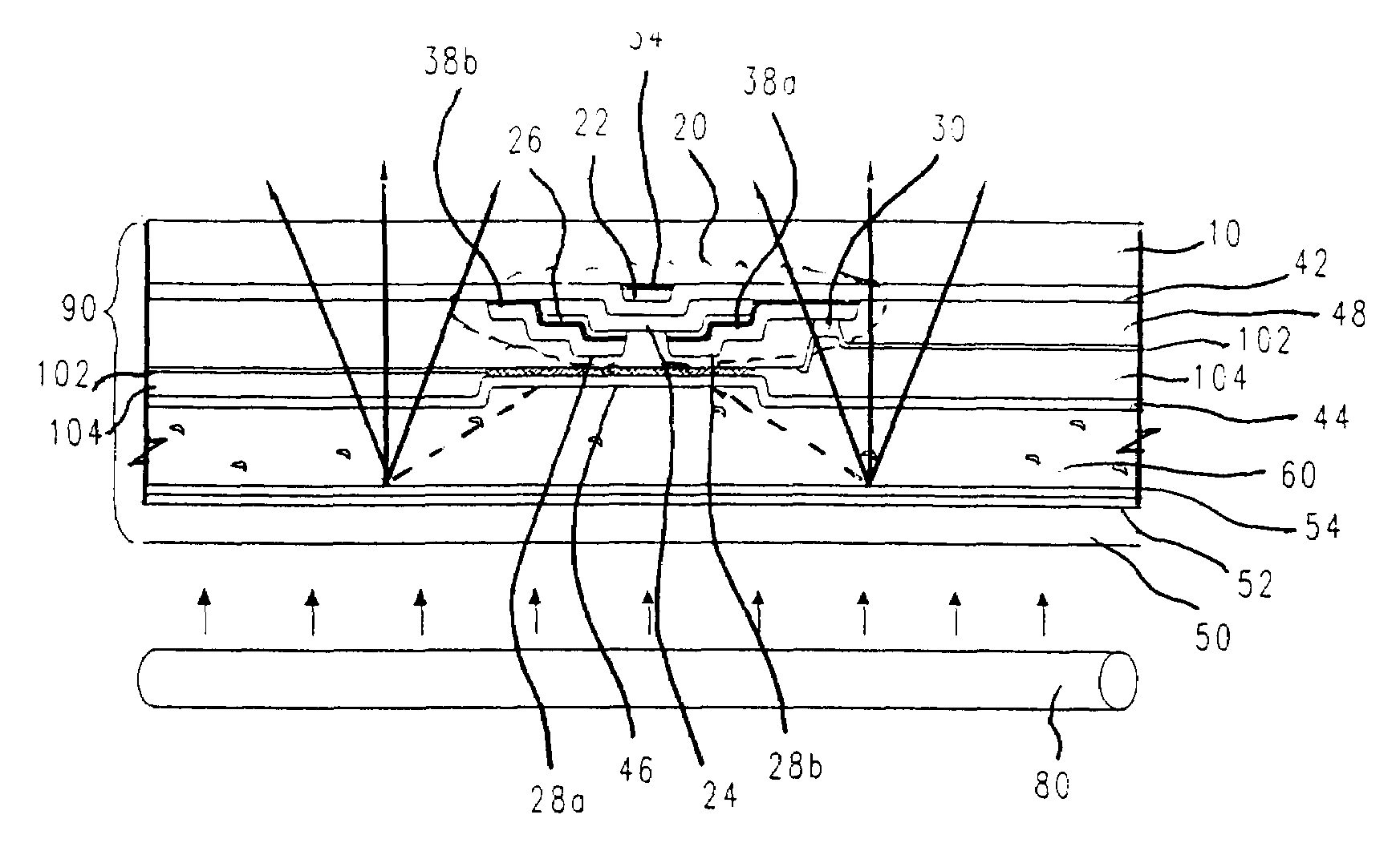
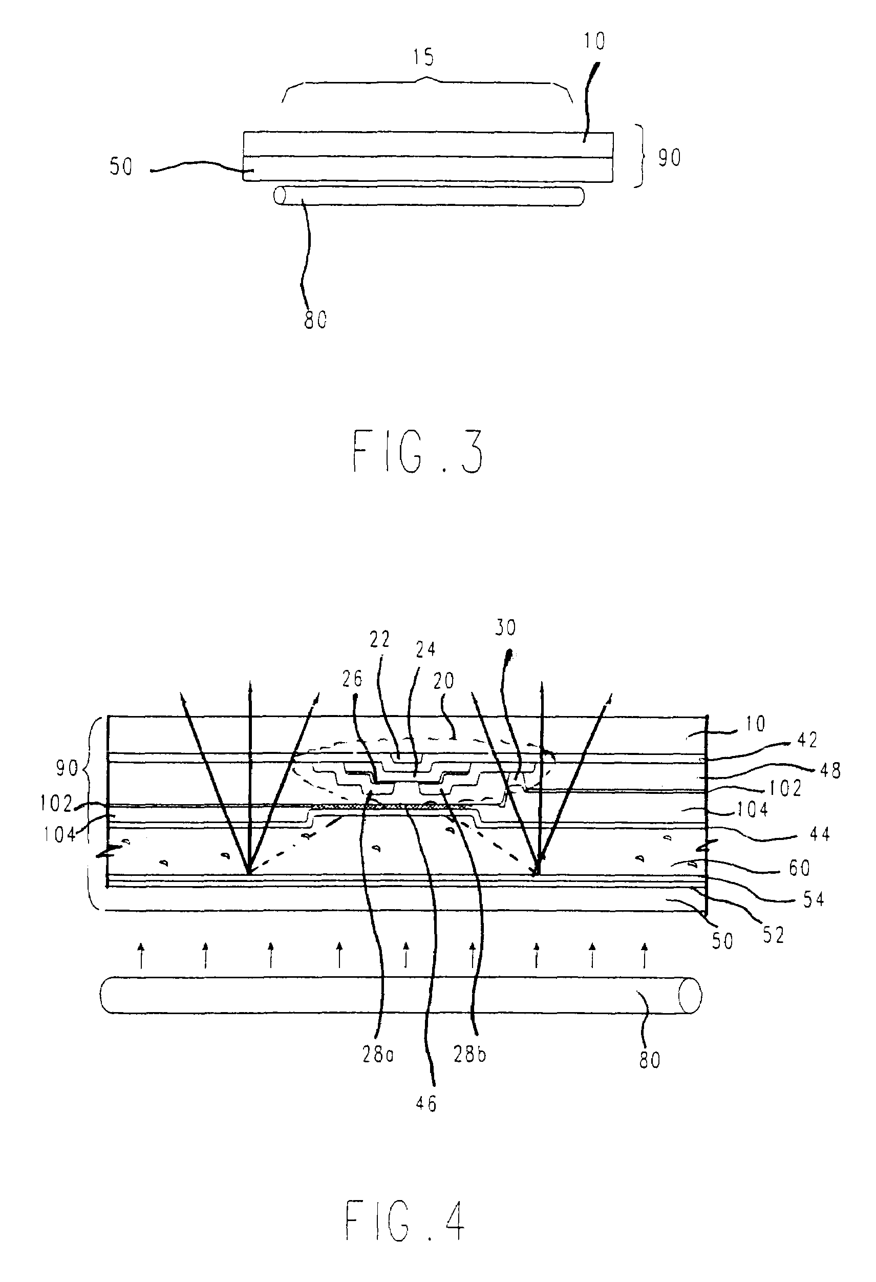
[0038]FIG. 3 is a schematic view illustrating a transmissive liquid crystal display device according to a preferred embodiment of the present invention. As shown in FIG. 3, the transmissive liquid crystal display device according to the preferred embodiment of the present invention includes a back light device 80 and a liquid crystal panel 90. The liquid crystal display panel 90 has a first substrate 10 and a second substrate 50 with a liquid crystal layer (not shown) interposed there-between. The liquid crystal display panel 90 is located over the back light device 80 so that a bottom surface of the second substrate 50 is adjacent to the back light device 80.

[0039]As the upper substrate, the first substrate 10 has pixel electrodes, thin film transistors as a switching element, color filters, and a black matrix disposed between...


PUM

PropertyMeasurementUnit
transparentaaaaaaaaaa
reflectanceaaaaaaaaaa
insulatingaaaaaaaaaa

Abstract

The present invention discloses a liquid crystal display device, comprising: a first upper substrate including: a) a switching element on the first upper substrate; b) a passivation film formed over the whole surface of the first upper substrate while covering the switching element; c) a pixel electrode on the passivation film; d) a black matrix formed on the passivation film and over the switching element; e) a color filter formed over the pixel electrode; and f) a first orientation film formed on the black matrix and the color filter and above the pixel electrode; a lower second substrate having a common electrode and a second orientation film, the orientation film formed on the common electrode; sealing the first and second substrates with a sealant and a liquid crystal layer interposed between the first upper and second lower substrates.

Description

CROSS REFERENCE[0001]This application claims the benefit of Korean Patent Application No. 1999-32448, filed on Aug. 7, 1999, under 35 U.S.C. § 119, the entirety of which is hereby incorporated by reference.BACKGROUND OF THE INVENTION[0002]1. Field of the Invention[0003]The present invention relates to a liquid crystal display (LCD) device and a method of manufacturing the same.[0004]2. Description of Related Art[0005]Recently, a liquid crystal display device adopts a structure wherein a color filter and a black matrix are formed over a thin film transistor array substrate to obtain a higher aperture ratio. The liquid crystal display device having such a structure (hereinafter, referred to simply as “the C / F and BM on array structure”) includes a top substrate, a bottom substrate, and a liquid crystal layer interposed between the two opposite substrates. The bottom substrate has an array of thin film transistors formed over the top surface of the bottom substrate, and both a black ma...

Claims


Application Information

Patent Timeline
Patent Type & Authority Patents(United States)
IPC IPC(8): G02F1/136G02F1/1333G09G3/36H01L29/04H01L31/00G02F1/1335G02F1/1362G09F9/00
CPCG02F1/136209G02F1/133553G02F1/1335
Inventor LEE, GUN-HEEKWAK, DONG-YOUNG
Owner LG DISPLAY CO LTD
Features
  • Generate Ideas
  • Intellectual Property
  • Life Sciences
  • Materials
  • Tech Scout
  • Unparalleled Data Quality
  • Higher Quality Content
  • 60% Fewer Hallucinations
Learn More