Metal oxide silicon transistor and semiconductor apparatus having high lambda and beta performances

a technology of metal oxide semiconductor and semiconductor apparatus, which is applied in the direction of pulse generator, pulse technique, electric pulse generator circuit, etc., can solve the problems of short effective channel length of mos transistor, designer may be required to compromise transistor performance, and differential amplifier circuit having a high performance needs a large channel area

Inactive Publication Date: 2007-08-28
RICOH ELECTRONIC DEVICES CO LTD
View PDF5 Cites 7 Cited by
  • Summary
  • Abstract
  • Description
  • Claims
  • Application Information

AI Technical Summary

Problems solved by technology

However, a MOS transistor with long effective channel length is unsuitable when for flowing a significant current.
As a result, a differential amplifier circuit having a high performance necessarily needs a large channel area.
Thus, a designer may be required to compromise transistor performance to achieve limited channel size.

Method used


Image

  • Metal oxide silicon transistor and semiconductor apparatus having high lambda and beta performances
  • Metal oxide silicon transistor and semiconductor apparatus having high lambda and beta performances
  • Metal oxide silicon transistor and semiconductor apparatus having high lambda and beta performances

Examples


Embodiment Construction

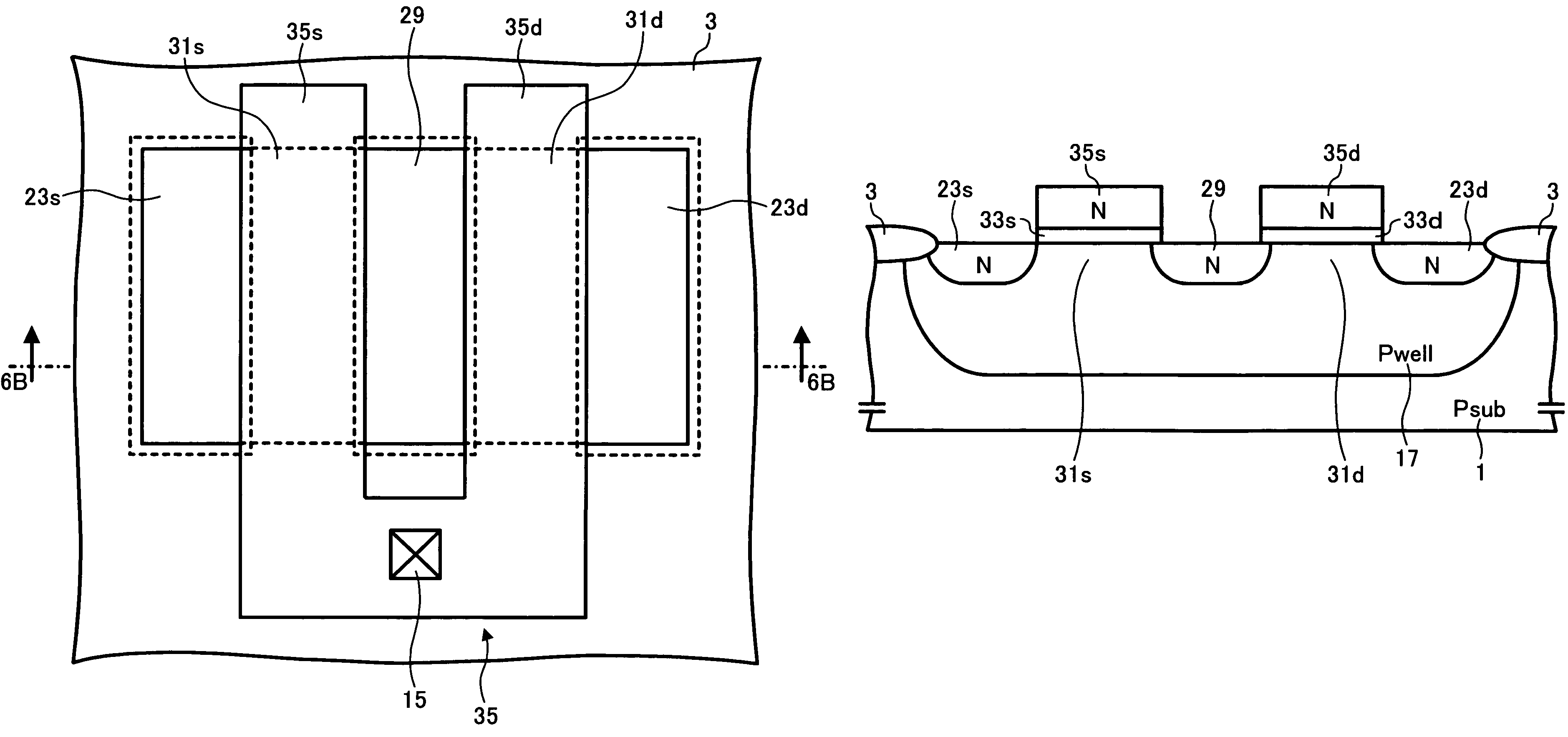
[0040]Referring now to the drawings, wherein like reference numerals designate identical or corresponding parts throughout several views, in particular to FIGS. 1A and 1B, an exemplary embodiment of the present invention includes a LOCOS oxide film 3 formed on a surface of a P-type semiconductor substrate 1 in order to separate an element device formation region in a Pch-MOS transistor. An N-well region 5 is preferably formed in the element device formation region of the semiconductor substrate 1. A gate oxide film 9 made of silicon is formed on a channel region 7 on a surface of the N-well region 5. An annular gate electrode 11 made of poly-silicon having implanted P-type impurity is preferably formed on the gate oxide film 9 while extending to the LOCOS oxide film 3. A source 13s and a drain 13d each receiving implantation of P-type impurity are preferably formed at both sides of the channel region 7 on the surface of the N-well region 5. An ohmic contact region 15 may be formed o...


PUM


Abstract

A semiconductor apparatus includes a MOS transistor having a semiconductor substrate providing as a channel region between a source and a drain. A gate electrode is formed on the semiconductor substrate via a gate oxide film. A threshold voltage of the source side region of the MOS transistor is higher than that of the drain side region in a longitudinal direction of the channel region so that a saturation drain current can be constant and a λ performance can be improved while suppressing channel width and length.

Description

[0001]This application claims priority under 35 U.S.C. § 119 to Japanese Patent Application No. 2003-041196, filed on Feb. 19, 2003, the entire contents of which are herein incorporated by reference.COPYRIGHT NOTICE[0002]A portion of the disclosure of this patent document contains material which is subject to copyright protection. The copyright owner has no objection to the facsimile reproduction by anyone of the patent document or the patent disclosure, as it appears in the Patent and Trademark Office patent file or records, but otherwise reserves all copyright rights whatsoever.BACKGROUND[0003]1. Field of the Invention[0004]The present specification relates generally to a MOS (Metal Oxide Semiconductor) transistor and a semiconductor apparatus employing a MOS transistor, and more particularly to a MOS transistor and such a semiconductor apparatus having various threshold voltages.[0005]2. Discussion of the Related Art[0006]It is known that a MOS transistor can be operated in a sat...

Claims


Application Information

Patent Timeline
Patent Type & Authority Patents(United States)
IPC IPC(8): H01L29/80H01L31/112H01L21/8234H01L21/8238H01L27/088H01L27/092H01L29/10H01L29/423H01L29/49H01L29/78H03K3/03
CPCH01L21/82345H01L21/823462H01L21/823842H01L27/088H01L27/092H01L29/1045H01L29/42368H01L29/4983H03K3/0315
Inventor NEGORO, TAKAAKISHIMIZU, AKIRA
Owner RICOH ELECTRONIC DEVICES CO LTD
Why Eureka
Try Eureka