Semiconductor package and method for manufacturing the same

a semiconductor and package technology, applied in the direction of semiconductor/solid-state device details, semiconductor devices, electrical devices, etc., can solve the problems of difficult to obtain semiconductor elements with stably operating and extended life, insufficient sealing properties, moisture resistance, chemical resistance or other properties, etc., to achieve excellent sealing properties, reduce the effect of reducing the number of process steps

Inactive Publication Date: 2007-09-25
FUJIKURA LTD
View PDF11 Cites 42 Cited by
  • Summary
  • Abstract
  • Description
  • Claims
  • Application Information

AI Technical Summary

Benefits of technology

[0016]An object of the invention is to provide a semiconductor package that exhibits excellent sealing property, moisture resistance, or chemical resistance in order to ensure a stable operation and an extended life of an element.
[0017]Another object of the invention is to provide a method for manufacturing such a semiconductor package having a good sealing property, moisture resistance, or chemical resistance without major increase in additional steps.

Problems solved by technology

A synthetic resin is typically used for the sealing material 47, and some synthetic resins do not necessarily exhibit sufficient sealing property, moisture resistance, chemical resistance, or other properties.
Consequently, a semiconductor element that stably operates and has an extended life is difficult to obtain.

Method used


Image

  • Semiconductor package and method for manufacturing the same
  • Semiconductor package and method for manufacturing the same
  • Semiconductor package and method for manufacturing the same

Examples


first embodiment

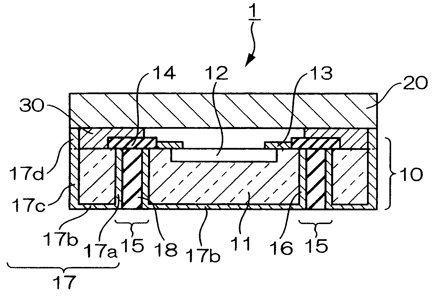
[0034]FIG. 1 is a cross-sectional view of a first embodiment of a semiconductor package according to an exemplary embodiment of the invention. A semiconductor package 1 according to this embodiment includes a first substrate 10 on which a functional element 12 is formed and a second substrate 20 that is a cap substrate, and the first substrate 10 and the second substrate 20 are bonded by the sealing material 30.

[0035]The first substrate 10 includes a semiconductor substrate 11. The functional element 12, and first wirings 13 and pads 14 connected thereto are provided on one side of the semiconductor substrate 11, and through-hole interconnections 15 electrically connect the other side of the semiconductor substrate 11 and the pads 14. The through-hole interconnections 15 are formed by filling, via an insulating film A 17a, a first conductive material 18 inside microholes (holes) 16 that penetrate the semiconductor substrate 11.

[0036]In this embodiment, the insulating film A 17a is f...

second embodiment

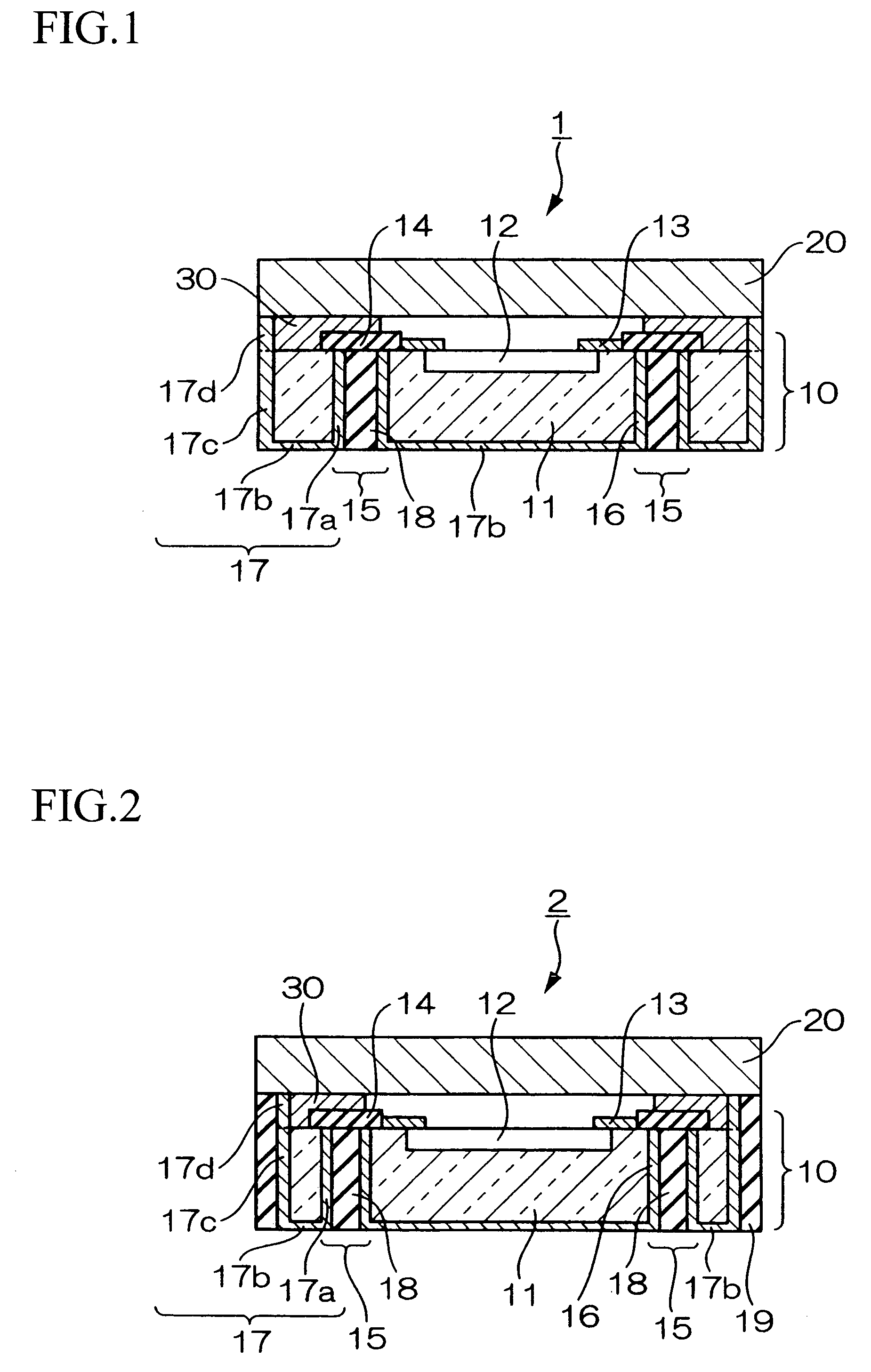
[0041]FIG. 2 is a cross-sectional view of a first embodiment of a semiconductor package 2 according to a second exemplary embodiment of the invention. The semiconductor package 2 according to this embodiment has a similar internal structure as that of the semiconductor package 1 of the first embodiment. In other words, the semiconductor package 2 includes a first substrate 10 on which a functional element 12 is formed and a second substrate 20 that is a cap substrate, and the first substrate 10 and the second substrate 20 are bonded by the sealing material 30. The first substrate 10 includes a semiconductor substrate 11. The functional element 12, and first wirings 13 and pads 14 connected thereto are provided on one side of the semiconductor substrate 11, and through-hole interconnections 15 electrically connect the other side of the semiconductor substrate 11 and the pads 14. The through-hole interconnections 15 are formed by filling a first conductive material 18 inside microhole...


PUM


Abstract

A semiconductor package includes: a first substrate including: a semiconductor base material having a first side and a second side; a functional element that is provided at the first side of the semiconductor base material; a first wiring; a pad that is electrically connected to the functional element via the first wiring; a through-hole interconnection that is electrically connected to the pad and is provided in a hole that is defined penetrating the semiconductor base material from the first side thereof to the second side thereof, the through-hole interconnection including a first insulating film and a first conductive material formed on the first insulating film; and a sealing material provided surrounding the functional element; a second substrate that is bonded to a first side of the first substrate via the sealing material.

Description

CROSS-REFERENCE TO RELATED APPLICATIONS[0001]This Application is based upon and claims the benefit of priority from Japanese Patent Application No. 2004-194663, filed Jun. 30, 2004 in the Japanese Patent Office, the disclosure of which is incorporated herein in its entirety by reference.BACKGROUND OF THE INVENTION[0002]1. Field of the Invention[0003]The invention relates to a packaging structure for a semiconductor package having a functional element and a through-hole interconnection that connects the front side and the back side, and to a method for manufacturing thereof.[0004]2. Description of Related Art[0005]In a related art technique for packaging a functional element such as a semiconductor light receiving sensor, a functional element is typically contained in a sealing container made of a ceramic or a resin and is then sealed. An example of this related art technique is shown in FIG. 5 (see Japanese Unexamined Patent Application, First Publication No. 2001-351997, for exampl...

Claims


Application Information

Patent Timeline
Patent Type & Authority Patents(United States)
IPC IPC(8): H01L23/04H01L23/02H01L23/48H01L23/52
CPCH01L27/14618H01L31/0203H01L2224/94H01L21/76898H01L23/02H01L31/02
Inventor TOMITA, MICHIKAZUSUEMASU, TATSUOHIRAFUNE, SAYAKA
Owner FUJIKURA LTD
Why Eureka
Try Eureka