Test circuit for memory

a test circuit and memory technology, applied in the field of test circuits for memory, can solve the problems of increasing the area due, changing the test contents, and the test of the memory itself for a ram test command also become a problem

Inactive Publication Date: 2007-09-25
RENESAS ELECTRONICS CORP
View PDF15 Cites 12 Cited by
  • Summary
  • Abstract
  • Description
  • Claims
  • Application Information

AI Technical Summary

Benefits of technology

[0015]A test circuit for a memory of the present invention is constructed so that, in a test circuit which is incorporated into a semiconductor integrated circuit together with the memory, the test circuit has a test signal generating circuit for generating a test signal for said memory, and a control circuit for conducting control of said test signal generating circuit, and a test setting mode and a test execution mode are switched to each other in accordance with a first control signal input from outside, and an initial data of the test signal and a control data for controlling said test signal generating circuit, which are input to said test signal generating circuit in said test setting mode, and a control data to said control circuit are input serially from an identical terminal.
[0016]In the present invention, since it is constructed so that the test setting mode and the test execution mode are switched to each other in accordance with the first control signal input from outside, and the initial data of the test signal and the control data for controlling said test signal generating circuit, which are input to said test signal generating circuit in said test setting mode, and the control data to said control circuit are input serially from the identical terminal, it is possible to change the test contents of the memory by means of a small number of external terminals.

Problems solved by technology

However, in the general BIST circuit, a sequencer is provided inside the memory test circuit, and since the sequencer controls test contents, the test contents are fixed, and it is impossible to change the test contents after a design of the LSI.
Accordingly, in case that a bit width of a data input or a data output is large or in case that a plurality of memories is integrated, there is a defect that a number of terminals for a test are required, which becomes impractical.
On the other hand, in the BIST circuit as shown in FIG. 11, the increase of an area due to the incorporation of the memory for a RAM test command inside the LSI, and a test of the memory itself for a RAM test command also become a problem.
In the BIST circuit proposed in the patent document 2, although the increase of an area due to the addition of the memory for a RAM test command does not occur, the increase of an area due to signal lines or the like for drawing a program from the scan path register inside the LSI, which is used as the substitution for the memory for a RAM test command, and the deterioration of a wiring characteristic during layout become a problem.
Also, since these test circuits generate a test pattern from a program, there is a defect that, in the RAM test control circuit and the test pattern generator, a circuit for conducting the decode of a program, the generation of a control signal of the RAM or the like is required, and a circuit size becomes larger.

Method used


Image

  • Test circuit for memory
  • Test circuit for memory
  • Test circuit for memory

Examples


Embodiment Construction

[0029]Hereinafter, referring to drawings, the present invention will be explained further in detail based on embodiments of the present inventions.

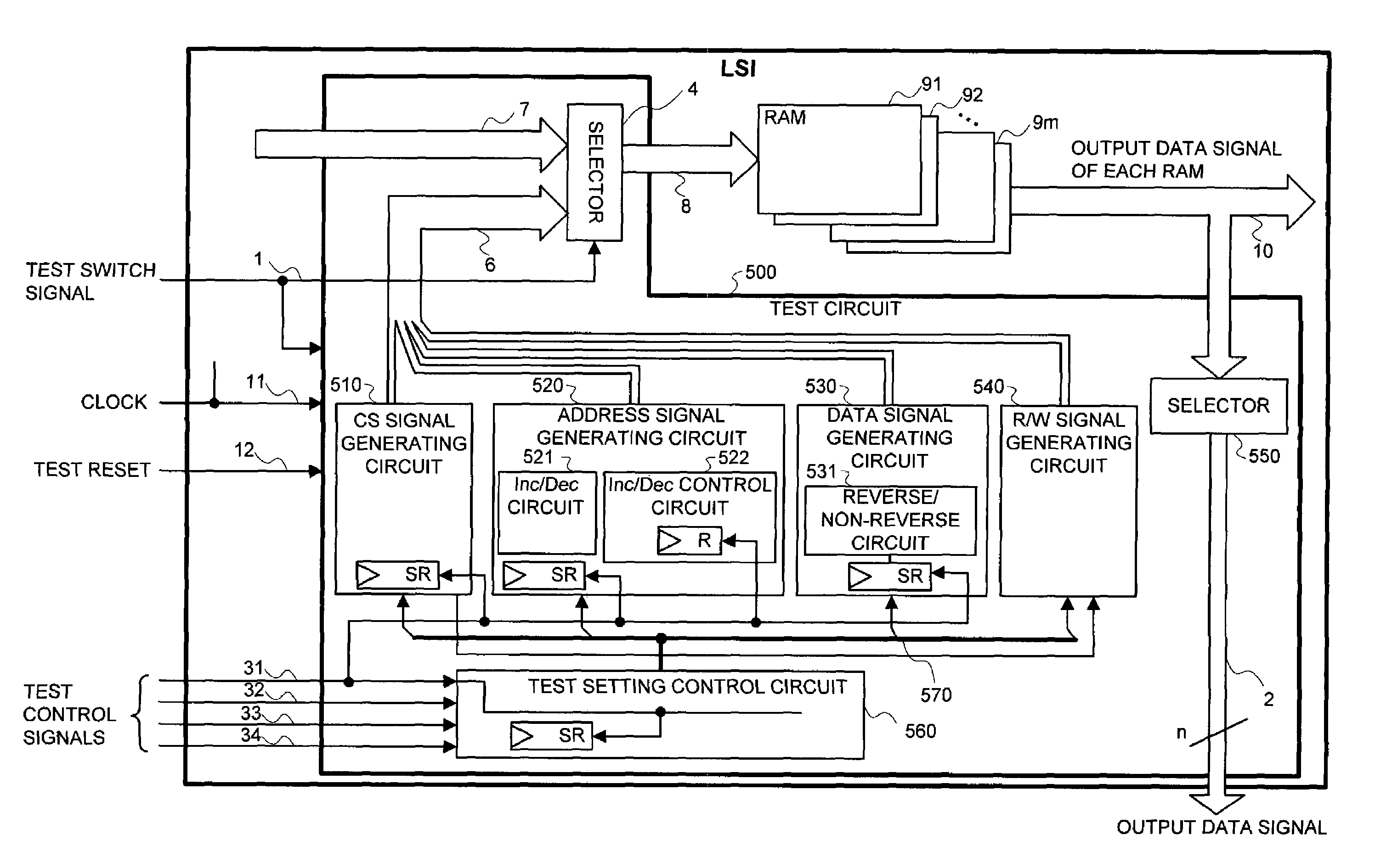
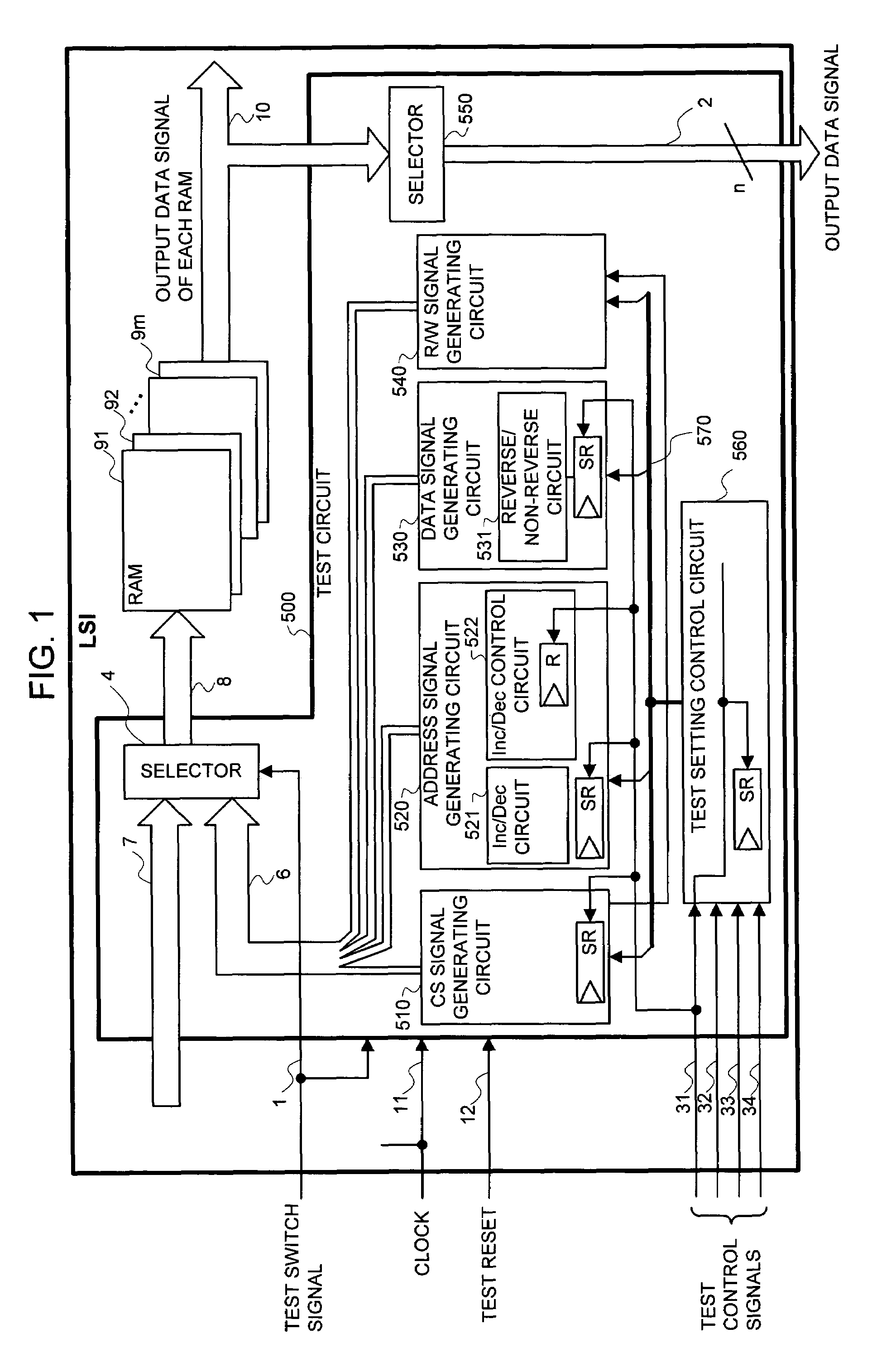
[0030]FIG. 1 shows an arrangement of an LSI having a test circuit for a memory in relation to an embodiment of the present invention. The LSI to which the test circuit for the memory of the present invention is applied has a plurality of RAM 91-9m and a test circuit 500.

[0031]An output 6 of the test circuit 500 is a data signal, an address signal, a chip select (CS) signal and a read / write (R / W) signal that are input signals to each of the RAM 91-9m during a test, and is connected to one of the inputs of a selector 4, and to the other of the inputs of the selector 4, the data signal, the address signal, the CS signal and the R / W signal are connected as an input signal 7 to each of the RAM 91-9m during a normal operation.

[0032]The selector 4 switches the signals 6 and 7 to each other by means of a test switch signal 1 input from an externa...


PUM


Abstract

Each signal generating circuit for generating a CS signal, an address signal, a data signal or an R/W signal of a memory to be tested, and a test setting control circuit for generating a control data of these signal generating circuits are provided. The signal generating circuits and the test setting control circuit have shift registers, and a control data and a test data are serially input to these shift registers from external terminals.

Description

BACKGROUND OF THE INVENTION[0001]The present invention relates to a test circuit for a memory, and especially, to a test circuit for a memory of a semiconductor integrated circuit in which a memory and a logic section are mixedly loaded on one semiconductor chip.[0002]In recent years, various kinds of LSIs in which a memory is mixedly loaded in a logic section such as an ASIC and a microprocessor have been proposed. In this kind of LSI, a normal operation of the memory is controlled by a signal from the logic section, and for example, when a read command is issued from the logic section, the memory outputs a data of a selected address to the logic section. Similarly, the memory outputs the data of the selected address to the logic section. In this kind of LSI, since to conduct a test of the memory through the complicated logic section is impractical, various exclusive test circuits for conducting a test of the memory have been proposed.[0003]FIG. 10 is a view showing an arrangement ...

Claims


Application Information

Patent Timeline
Patent Type & Authority Patents(United States)
IPC IPC(8): G11C29/10G11C29/40G01R31/28G01R31/3185G11C29/00G11C29/12G11C29/14H01L21/822H01L27/04
CPCG11C29/14G11C29/00
Inventor KAWASAKI, TATSUYA
Owner RENESAS ELECTRONICS CORP
Why Eureka
Try Eureka