Component mounting method

a technology of component mounting and mounting method, which is applied in the direction of metal working apparatus, manufacturing tools, printed circuit manufacturing, etc., can solve the problem that the apparatus is not always suitable for bonding a pair of semiconductor chips, and achieve the effect of effective component mounting operation

Active Publication Date: 2007-10-16
PANASONIC CORP
View PDF13 Cites 6 Cited by
  • Summary
  • Abstract
  • Description
  • Claims
  • Application Information

AI Technical Summary

Benefits of technology

[0007]This invention has been made in view of the above circumstances, and an object of the invention is to provide a component mounting apparatus and a component bonding method which can effectively perform a component mounting operation to manufacture semiconductor devices having a chip-on-chip structure.
[0018]According to the invention, in the component mounting operation that the second component is mounted on the first component, the first component is transported to the mounting stage by the component transporting unit, and then the second component transferred from the component transporting unit is mounted on the first component by the mounting head. By this construction, it is possible to effectively perform component mounting operation for manufacturing semiconductor devices having COC structure.

Problems solved by technology

However, since the component mounting apparatus shown in the above patent publication is configured for applications in which semiconductor chips are transported and mounted on a board which has a relatively large size such that the board can be easily handled, the apparatus is not always suitable to bond a pair of semiconductor chips having almost the same size to each other.

Method used


Image

  • Component mounting method
  • Component mounting method
  • Component mounting method

Examples


embodiment 1

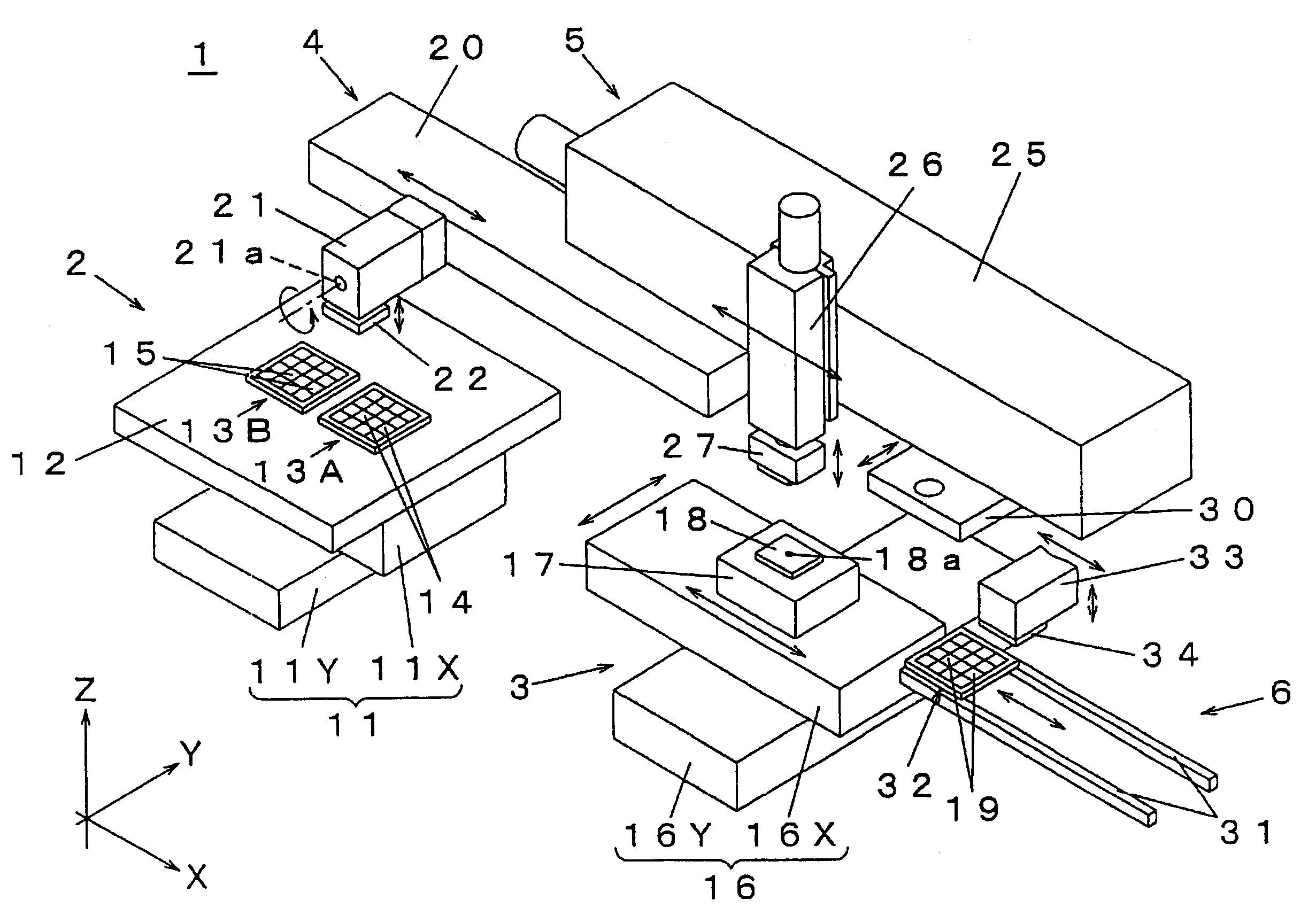
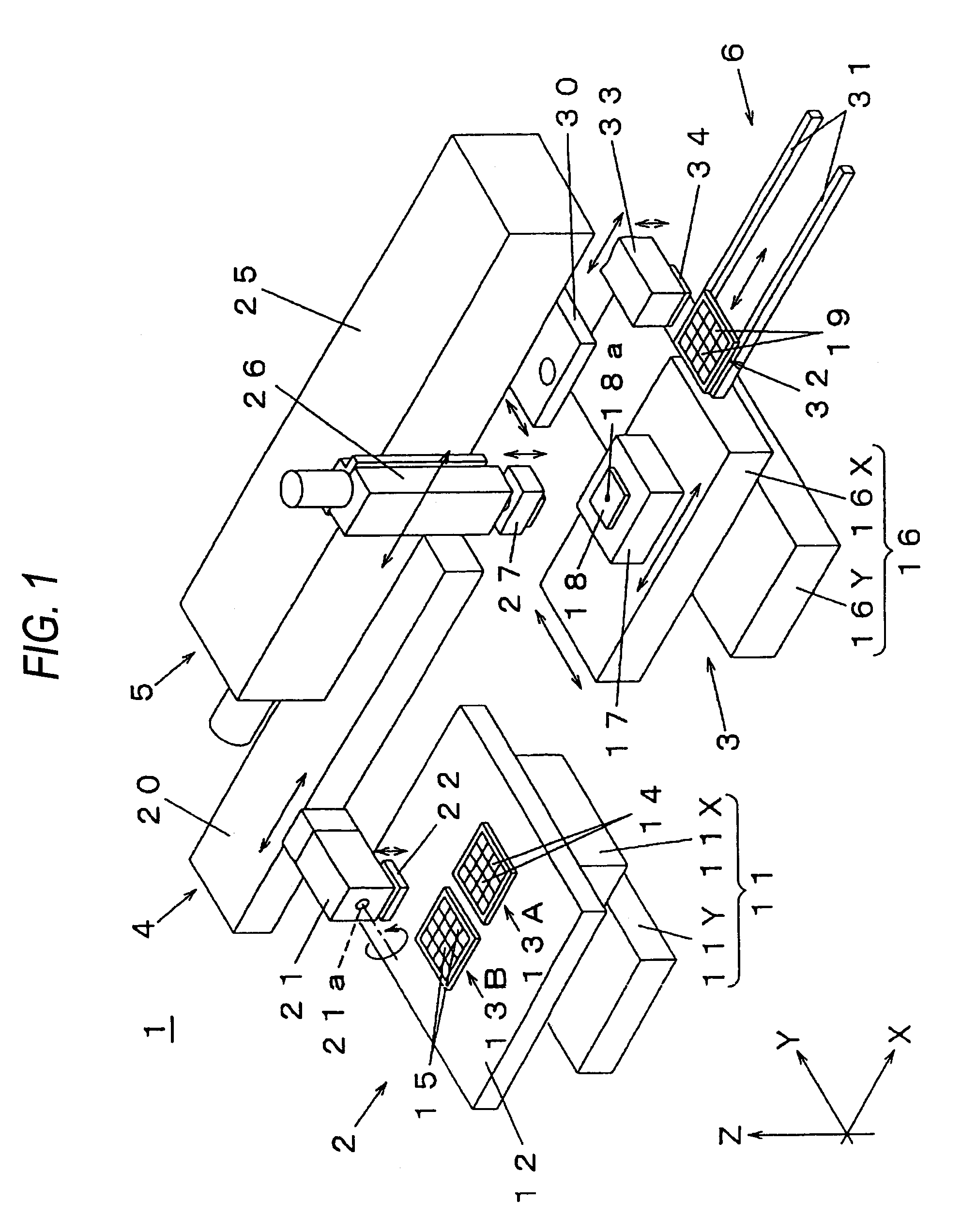
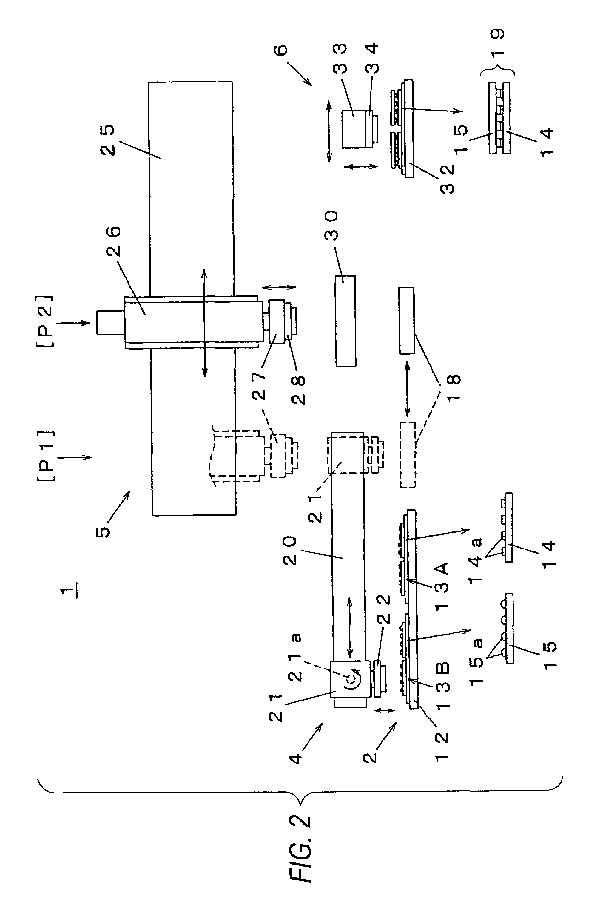
[0027]FIG. 1 is a perspective view showing a component mounting apparatus according to Embodiment 1 of the present invention; FIG. 2 is a front view showing the component mounting apparatus according to Embodiment 1 of the present invention; and FIGS. 3A through 4D are process explanatory views showing a component mounting method according to Embodiment 1 of the present invention.

[0028]Referring to FIGS. 1 and 2, the structure of a component mounting apparatus 1 will be described below. The component mounting apparatus 1 is served for manufacturing integrated components (semiconductor devices) having COC structure made by mounting semiconductor chips with substantially the same size in a directly stacked manner. In FIG. 1, the component mounting apparatus 1 is configured so that a component feeding unit 2 and a component positioning unit 3 are arranged serially in X direction (component transportation direction), and above these units, a component transporting unit 4 and a component...

embodiment 2

[0051]FIG. 5 is a perspective view showing a component mounting apparatus according to Embodiment 2 of the present invention; FIG. 6 is a front view showing the component mounting apparatus according to Embodiment 2 of the present invention; and FIGS. 7A and 8D are explanatory views showing process of a component mounting method according to Embodiment 2 of the present invention.

[0052]A component mounting apparatus 1A shown in FIG. 5 and 6 has a construction where the component carrying-out unit 6 and the component transporting head 33 are eliminated from the component mounting apparatus 1. The structure constituted by the component storing unit 2, the component positioning unit 3, the component transporting unit 4 and the component mounting unit 5 is similar to the component mounting apparatus 1. In Embodiment 2, the component mounting apparatus 1A is configured so that the integrated component 19 formed by mounting the upper chip 15 on the lower chip 14 on the mounting stage 18 is...


PUM

PropertyMeasurementUnit
densityaaaaaaaaaa
sizeaaaaaaaaaa
timeaaaaaaaaaa

Abstract

In a component mounting apparatus in which integrated components having a chip-on-chip structure are formed by mounting upper chips on lower chips. The lower chips picked up from a component carrying-in unit by a component carrying-in head are placed on a mounting stage, and the upper chips picked up from a second component tray by a component transporting head are vertically flipped around a rotation axis and transferred to a mounting head at a component transferring position, then the upper chips held by the mounting head are descended and mounted by solder bonding on the lower chips held by the mounting stage at a component mounting position. Integrated components formed by mounting are carried out of the mounting stage by the component transporting head and stored in a first component tray in a component storing unit.

Description

BACKGROUND OF THE INVENTION[0001]1. Field of the invention[0002]This invention relates to a component mounting apparatus and a component mounting method in which another component is mounted on one component in a stacked manner.[0003]2. Related Art[0004]In field of manufacturing electronic devices, component mounting operations are performed such that semiconductor chips are mounted on a work like circuit boards etc. In such a component mounting operation, there are two operations: a transporting and placing operation where semiconductor chips in which connection terminals such as solder bumps are formed are picked up from a component feeding unit and placed on a board, and a bonding operation where the connection terminals of the semiconductors are bonded to circuit terminals on the board. For an apparatus to perform such component mounting operations, there is known conventionally a component mounting apparatus includes a component flipping mechanism which picks up semiconductor c...

Claims


Application Information

Patent Timeline
Patent Type & Authority Patents(United States)
IPC IPC(8): H05K3/30
CPCH05K13/0465H01L2224/75H01L2224/75745H01L2224/758H01L2924/01087Y10T29/53174H01L2924/07811Y10T29/49144Y10T29/4913H01L2924/00H05K13/04
Inventor ONOBORI, SHUNJIMINAMITANI, SHOZOHIRATA, SHUICHINAKANISHI, TOMOAKI
Owner PANASONIC CORP
Why Eureka
Try Eureka