Three dimensional twisted bitline architecture for multi-port memory

a multi-port memory and bitline technology, applied in the direction of digital storage, instruments, semiconductor devices, etc., can solve the problems of data contention on the common bl, potential rbl and wbl coupling noise, and simultaneous read and write operation difficult or potentially impossible, and achieve reliable differential sensing

Inactive Publication Date: 2007-10-23
IBM CORP
View PDF10 Cites 10 Cited by
  • Summary
  • Abstract
  • Description
  • Claims
  • Application Information

AI Technical Summary

Benefits of technology

[0011]The invention relates to an architecture for a memory array of multi-port cells that enables reliable differential sensing by creating common mode noise while simultaneously canceling the coupling level.

Problems solved by technology

This is because activating two or more WLs causes a data contention on the common BL.
Note that these read and write operation are simultaneously enabled, which causes a potential RBL and WBL coupling noise.
Over 250 mV coupling noise makes a simultaneous read and write operation difficult or potentially impossible.
However, this would increase the cell area significantly.
Note that this WBL coupling noise to the RBL is a unique problem that results from enabling a simultaneous read and write operation.
Note that a conventional BL twisting method is not applicable to cancel the noise, because of a single ended RBL and WBL configuration used in this array.

Method used


Image

  • Three dimensional twisted bitline architecture for multi-port memory
  • Three dimensional twisted bitline architecture for multi-port memory
  • Three dimensional twisted bitline architecture for multi-port memory

Examples


Embodiment Construction

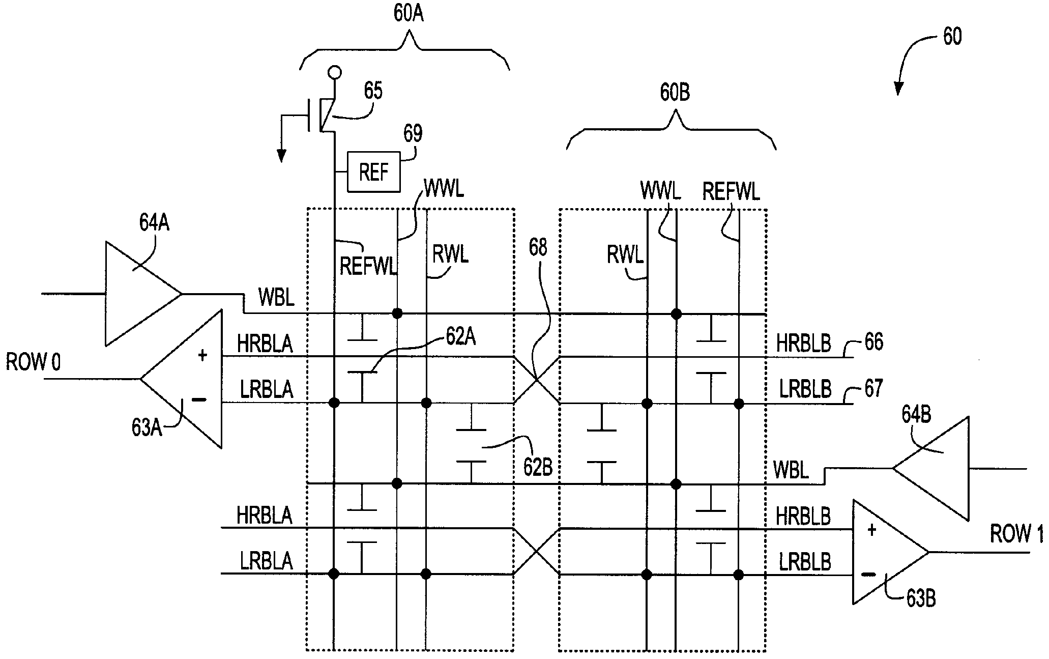
[0022]FIG. 6 shows a first method to overcome the problem described in the copending application Ser. No. 10 / 604,994, filed Aug. 29, 2003 and incorporated by reference in its entirety. A single memory array 60 comprises a plurality of 3 T gain cells arranged in a matrix. However, other memory cells, which have a read and write port, may be used to configure a memory array. The single memory array is further divided into two memory sections 60A and 60B. Each WBL is extended into the two memory sections 60A and 60B. On the other hand, each RBL 67 in a same column is divided into two local RBL (LRBLA and LRBLB). Each memory column further contains hierarchical read bitlines 66 (HRBLA and HRBLB) that do not connect to the cells. They are arranged over the LRBLA and LRBLB in a different wiring layer. LRBLA and LRBLB (line 67) are coupled to the HRBLB and HRBLA (line 66) respectively by vertically twisting structure 68.

[0023]The effect of the twisting structure 68 is that the two sections...


PUM


Abstract

A memory array of dual part cells has a pair of twisted write bitlines and a pair of twisted read bitlines for each column. The twist is made by alternating the vertical position of each bitline pair in each section of a column, with the result of generating common mode nose and of reducing differential mode noise.

Description

FIELD OF THE INVENTION[0001]This invention is related to Multi-port memory architecture. More particularly, this invention describes the improved architecture for a multi-port memory to enable a reliable differential sensing by creating a common noise while canceling the coupling level.BACKGROUND OF THE INVENTION[0002]Single port memory allows either a read or write operation for each cycle time. Typically, the single port memory uses either 6 transistor static memory cells (6 T SRAM) or a single 1-transistor dynamic cell (1T). FIG. 1-A shows a transistor level schematic for the typical 6 T SRAM cell 0. It consists of four NMOS transistors 1,2,5, and 6, and two PMOS transistors 3 and 4. The PMOSs 3 and 4 and NMOSs 5 and 6 configure a CMOS cross-coupled latch, which maintains a data bit as a storage element. The NMOSs 1 and 2 are used to couple the nodes 7 and 8 to the bitlines (BL and bBL) when a wordline WL is activated. This allows the data bit to be read or written from the BL an...

Claims


Application Information

Patent Timeline
Patent Type & Authority Patents(United States)
IPC IPC(8): G11C8/00
CPCG11C5/063G11C7/02G11C7/18G11C8/16G11C11/412G11C11/4097H01L27/11898H01L27/10894H01L27/11H01L27/1104H10B12/09H10B10/00H10B10/12
Inventor KIM, HOKIKIRIHATA, TOSHIAKI
Owner IBM CORP
Why Eureka
Try Eureka