Three dimensional twisted bitline architecture for multi-port memory

a multi-port memory and bitline technology, applied in the direction of information storage, static storage, digital storage, etc., can solve the problems of data contention on the common bl, potential rbl and wbl coupling noise, and difficulty or potential inability to perform simultaneous read and write operations, so as to reduce differential mode noise

Inactive Publication Date: 2011-02-08
INT BUSINESS MASCH CORP
View PDF10 Cites 7 Cited by
  • Summary
  • Abstract
  • Description
  • Claims
  • Application Information

AI Technical Summary

Benefits of technology

[0014]The present invention relates to a memory array architecture of multi-port cells that enables reliable differential sensing by creating common mode noise while simultaneously canceling the coupling level.
[0017]Embodiments of the present invention also provide a pair of twisted bitlines for both the read bitlines and the write bitlines. The twist is made by alternating the vertical position of each bit line pair in each section of a column, with the result of generating common mode nose and of reducing differential mode noise.

Problems solved by technology

This is because activating two or more WLs causes a data contention on the common BL.
Note that these read and write operation are simultaneously enabled, which causes a potential RBL and WBL coupling noise.
Over 250 mV coupling noise makes it difficult or potentially impossible for a simultaneous read and write operation.
However, this would increase the cell area significantly.
Note that this WBL coupling noise to the RBL is a unique problem that results from enabling a simultaneous read and write operation.
Note that a conventional BL twisting method is not applicable to cancel the noise, because of a single ended RBL and WBL configuration used in this array.

Method used


Image

  • Three dimensional twisted bitline architecture for multi-port memory
  • Three dimensional twisted bitline architecture for multi-port memory
  • Three dimensional twisted bitline architecture for multi-port memory

Examples


first embodiment

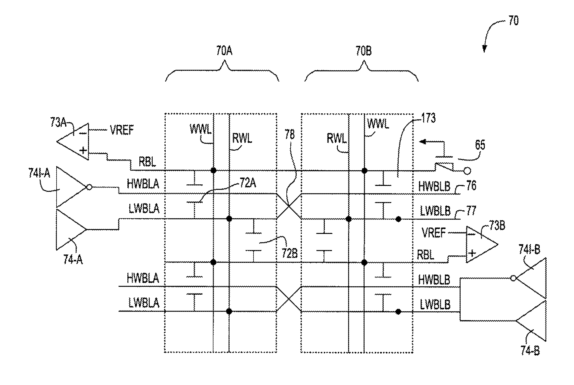
[0034]Unlike the first embodiment, each RBL is extended into two memory sections 70A and 70B. They are directly coupled to the corresponding sense amplifier 73 together with the other input VREF. On the other hand, each WBL in a column is divided into two local WBL (LWBLA and LWBLB). Each memory section of the column further contains a hierarchical write bitline (HWBLA and HWBLB). The HWBLA and HWLBLB are arranged over the LWBLA and LWBLB in another metal layer. LWBLA and LWBLB are coupled to the HWBLB and HWBLA respectively by vertically twisting them at the twisting area 78. The LWBLA and HWBLB in a row 0 are coupled to write drivers 74A and 74IA located at the edge of the memory section A.

[0035]Similarly, the LWBLA and HWBLB in a row 1 are coupled to the write drivers 74B and 74IB located at the edge of the memory section B. This interleaved circuit arrangement makes it easy to accommodate the write driver circuitry. Optionally, both all drivers 74A, 74IA, 74B and 74IB may be arr...

second embodiment

[0036]An advantageous feature of this invention is that the write drivers 74 and 74I drive the corresponding HWBLA connecting to LWBLB through vertical twist 78 and drive LWLBLA connecting to HWLBLB in the opposite direction (with the opposite polarity). Thus the opposite polarity of the signals received in the adjacent RBL cancels the coupling noise to the adjacent RBL 173. This is because half of the adjacent RBL 173 is close to LWBLA and the other half of the adjacent RBL 173 is close to LWBLB, where LWBLA and LWBLB swing in the opposite direction. This allows the RBL sensing operation by utilizing a constant RBL reference voltage VREF. The VREF voltage is set to a half level when the RBL discharges when the high data bit would be read out from the memory cell. This second embodiment has the following two disadvantages over the previous embodiment. Firstly, the number of the cells coupling to the RBL is 2× of that for the first method, because one RBL supports all the column. In ...


PUM


Abstract

Embodiments of the present invention provide a memory array of dual part cells and design structure thereof. The memory array has a pair of twisted write bit lines and a pair of twisted read bit lines for each column. The twist is made by alternating the vertical position of each bit line pair in each section of a column, with the result of generating common mode nose and of reducing differential mode noise.

Description

CROSS-REFERENCE TO RELATED APPLICATIONS[0001]This application is related to a US patent application entitled “Three Dimensional Twisted Bitline Architecture for Multi-port Memory”, to be issued as U.S. Pat. Ser. No. 7,286,437 on Oct. 23, 2007.FIELD OF THE INVENTION[0002]The present application is related to a multi-port memory architecture and related design structure thereof. More particularly, it relates to an improved architecture for a multi-port memory to enable a reliable differential sensing by creating a common noise while canceling the coupling level.BACKGROUND OF THE INVENTION[0003]Single port memory allows either a read or a write operation for each cycle time. Typically, the single port memory uses either 6 transistor static memory cells (6T SRAM) or a single 1-transistor dynamic cell (1T). FIG. 1-A shows a transistor level schematic for the typical 6T SRAM cell 0. It consists of four NMOS transistors 1, 2, 5 and 6, and two PMOS transistors 3 and 4. The PMOSs 3 and 4 and...

Claims


Application Information

Patent Timeline
Patent Type & Authority Patents(United States)
IPC IPC(8): G11C8/00
CPCG11C7/02G11C7/1075G11C7/18G11C8/16G11C11/412
Inventor KIM, HOKIKIRIHATA, TOSHIAKI
Owner INT BUSINESS MASCH CORP
Why Eureka
Try Eureka