Integrated nanotube and field effect switching device
What is AI technical title?
AI technical title is built by Patsnap AI team. It summarizes the technical point description of the patent document.
a nanotube and field effect technology, applied in nanoelectromechanical switches, pulse techniques, instruments, etc., can solve the problems of high power consumption, density and operation speed of mos digital circuits, and limited density of bipolar digital integrated circuits
Active Publication Date: 2007-10-30
NANTERO
View PDF164 Cites 15 Cited by
Summary
Abstract
Description
Claims
Application Information
AI Technical Summary
This helps you quickly interpret patents by identifying the three key elements:
Problems solved by technology
Method used
Benefits of technology
Problems solved by technology
However, the density of bipolar digital integrated circuits is limited by their high power consumption and the ability of packaging technology to dissipate the heat produced while the circuits are operating.
The density and operating speed of MOS digital circuits are still limited by the need to dissipate the heat produced when the device is operating.
Digital logic integrated circuits constructed from bipolar or MOS devices do not function correctly under conditions of high heat or heavy radiation.
As leakage current increases, the operating temperature of the device rises, the power consumed by the circuit increases, and the difficulty of discriminating the off state from the on state reduces circuit reliability.
Conventional digital logic circuits also short internally when subjected to heavy radiation because the radiation generates electrical currents inside the semiconductor material.
It is possible to manufacture integrated circuits with special devices and isolation techniques so that they remain operational when exposed to heavy radiation, but the high cost of these devices limits their availability and practicality.
In addition, radiation hardened digital circuits exhibit timing differences from their normal counterparts, requiring additional design verification to add radiation protection to an existing design.
Integrated circuits constructed from either bipolar or FET switching elements are volatile.
Alternative solutions to avoid losing information in volatile digital circuits, such as battery backup, also add cost and complexity to digital designs.
Method used
Image
Click on the blue label to locate the original text in one second.
Reading with bidirectional positioning of images and text.
Examples
Embodiment Construction
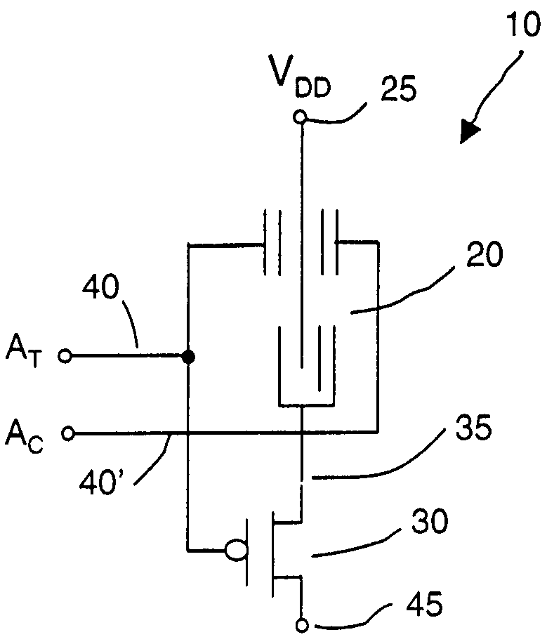
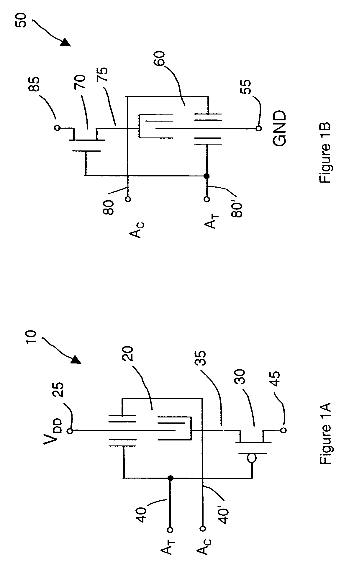
[0057]Embodiments of the invention provide switching elements with a conductive channel that has both a nanotube component and a field effect semiconductor component. Preferred embodiments of the invention provide integrated hybrid logic devices that use nanotube switching elements in combination with field effect devices resembling field effect transistors (FETs). The integrated devices are referred to herein as NT-FET devices. The NT-FET devices of preferred embodiments form an NT-FET device family. The devices in the NT-FET device family can be used as switching elements and to implement any desired logic function or logical device, such as an inverter. In certain embodiments, an NT-FET device includes a MOSFET, e.g., a p-channel FET (PFET) or an n-channel FET (NFET), placed in series with a nanotube switching element connected to a source (VDD or GND). In preferred embodiments, the gate of the FET is logically tied to a control input of the nanotube switching element. In some em...
PUM
Abstract
Hybrid switching devices integrate nanotube switching elements with field effect devices, such as NFETs and PFETs. A switching device forms and unforms a conductive channel from the signal input to the output subject to the relative state of the control input. In embodiments of the invention, the conductive channel includes a nanotube channel element and a field modulatable semiconductor channel element. The switching device may include a nanotube switching element and a field effect device electrically disposed in series. According to one aspect of the invention, an integrated switching device is a four-terminal device with a signal input terminal, a control input terminal, a second input terminal, and an output terminal. The devices may be non-volatile. The devices can form the basis for a hybrid NT-FET logic family and can be used to implement any Boolean logic circuit.
Description
CROSS-REFERENCE TO RELATED APPLICATIONS[0001]This application claims priority under 35 U.S.C. § 119(e) to U.S. Provisional Pat. Apl., Ser. No. 60 / 581,015, filed on Jun. 18, 2004, entitled Nonvolatile Carbon Nanotube Logic (NLOGIC) and CMOS Inverter, which is incorporated herein by reference in its entirety.[0002]This application is related to the following applications:[0003]U.S. patent application Ser. No. 10 / 917,794, filed on Aug. 13, 2004, entitled Nanotube-Based Switching Elements, now Publication No. 2005 / 0035367;[0004]U.S. patent application Ser. No. 10 / 918,085, filed on Aug. 13, 2004, entitled Nanotube-Based Switching Elements With Multiple Controls, now U.S. Pat. No. 6,990,009;[0005]U.S. patent application Ser. No. 10 / 918,181, filed on Aug. 13, 2004, entitled Nanotube Device Structure And Methods Of Fabrication, now U.S. Pat. No. 7,071,023;[0006]U.S. patent application Ser. No. 10 / 917,893, filed on Aug. 13, 2004, entitled Nanotube-Based Switching Elements And Logic Circuits,...
Claims
Application Information
Patent Timeline
Application Date:The date an application was filed.
Publication Date:The date a patent or application was officially published.
First Publication Date:The earliest publication date of a patent with the same application number.
Issue Date:Publication date of the patent grant document.
PCT Entry Date:The Entry date of PCT National Phase.
Estimated Expiry Date:The statutory expiry date of a patent right according to the Patent Law, and it is the longest term of protection that the patent right can achieve without the termination of the patent right due to other reasons(Term extension factor has been taken into account ).
Invalid Date:Actual expiry date is based on effective date or publication date of legal transaction data of invalid patent.

