Small signal amplifier with large signal output boost stage

a small signal amplifier and boost stage technology, applied in the field of amplifiers, can solve the problems of overdrive of output and inability to deliver the current demanded by load, and achieve the effect of simplifying the biasing and lowing the low power operation

Active Publication Date: 2007-10-30
ANALOG DEVICES INC
View PDF6 Cites 3 Cited by
  • Summary
  • Abstract
  • Description
  • Claims
  • Application Information

AI Technical Summary

Benefits of technology

[0007]The present amplifier circuit includes a small signal amplifier and a large signal output boost stage connected between first and second power supply rails. The small signal amplifier receives first and second input signals at respective input nodes and provides an output signal at an output node to which a load is connected. When the difference voltage between the input signals is less than a predetermined threshold (i.e., small signal), the output signal varies approximately linearly with the difference voltage. However, when the difference voltage is greater than the predetermined threshold (i.e., large signal), a rail-to-rail large signal output boost stage connected to the output node is arranged to drive the output node close to the first or second supply rail as needed to provide the current demanded by the load. The large signal output boost stage is off in small signal conditions, simplifying its biasing and allowing low power operation when only small signals are present. But the output stage comes on rapidly and transfers maximum charge to the load under large signal conditions. In this way, the present amplifier circuit supplies load currents that would otherwise overload the small signal amplifier.

Problems solved by technology

However, the desired small signal response may cause the output to be overdriven when large amounts of charge are called for, and thus unable to deliver the currents demanded by the load.

Method used


Image

  • Small signal amplifier with large signal output boost stage
  • Small signal amplifier with large signal output boost stage
  • Small signal amplifier with large signal output boost stage

Examples


Embodiment Construction

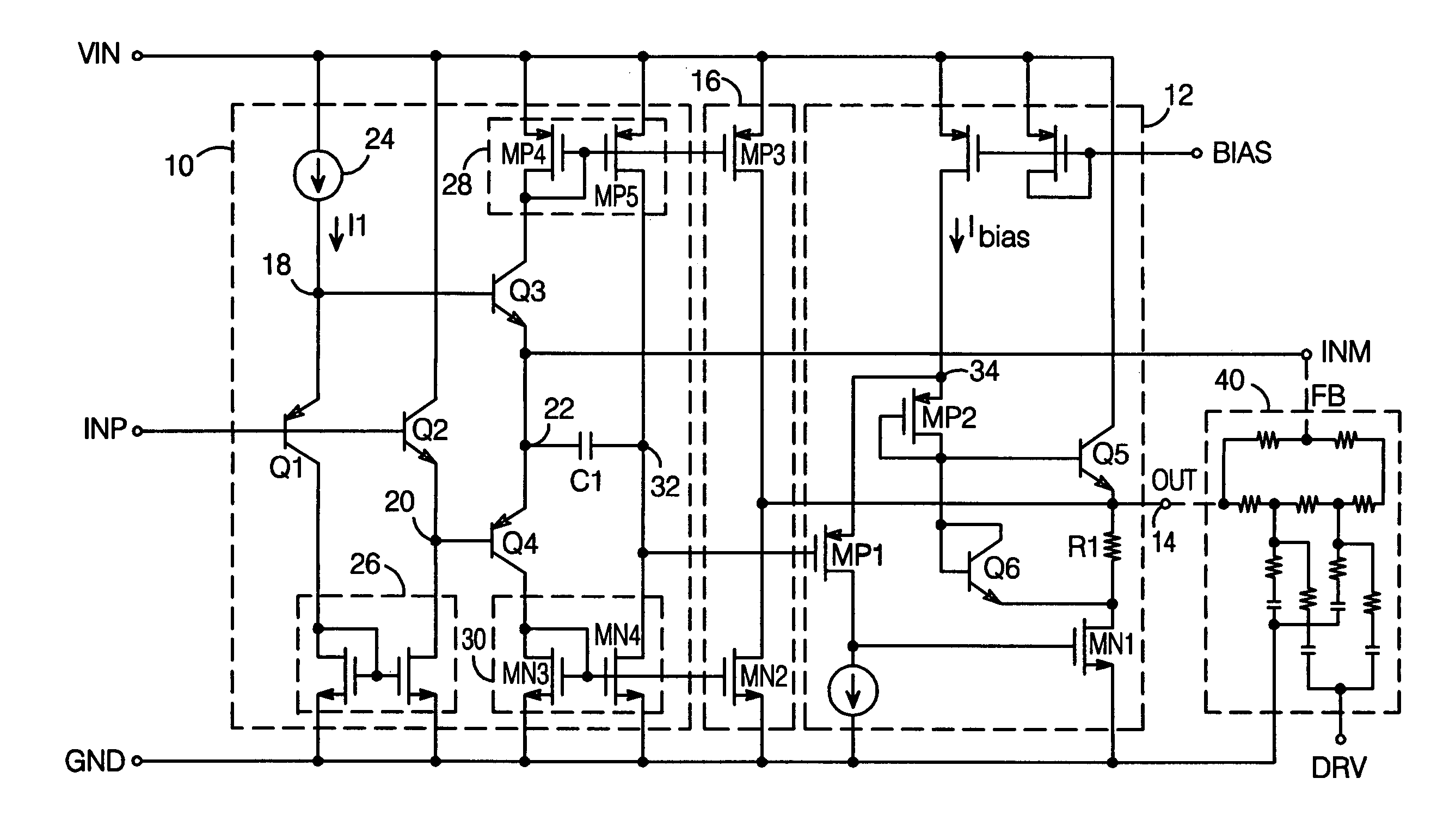
[0012]The present invention is an amplifier circuit capable of providing an accurate small signal response, and of supplying large currents when a large signal response is called for by the load being driven. This is accomplished by combining a small signal amplifier with a large signal output boost stage.

[0013]An exemplary embodiment of the present amplifier circuit is shown in FIG. 1. The amplifier circuit includes a small signal amplifier comprising a first stage 10 and an output stage 12 which drives an output node 14, and a large signal output boost stage 16 which is also connected to drive output node 14. The amplifier circuit is connected between first and second power rails, labeled in FIG. 1 as VIN and GND, though both rails could be at non-zero potentials.

[0014]The small signal amplifier is suitably configured as a current feedback amplifier. Here, first stage 10 comprises first and second transistors (Q1, Q2) of opposite polarity; Q1 and Q2 are shown as bipolar transistor...


PUM


Abstract

A small signal amplifier with a large signal output boost stage are connected between first and second supply rails. The small signal amplifier receives first and second input signals and provides an output signal at an output node which drives a load. Under small signal conditions, the output signal varies approximately linearly with the difference voltage. However, under large signal conditions, a rail-to-rail large signal output boost stage connected to the output node is arranged to drive the output node close to the first or second supply rail as needed to provide the current demanded by the load. The large signal output boost stage is off in small signal conditions, but comes on rapidly and transfers maximum charge to the load under large signal conditions.

Description

RELATED APPLICATIONS[0001]This application claims the benefit of provisional patent application No. 60 / 647,299 to Brokaw, filed Jan. 25, 2005, and of provisional patent application No. 60 / 741,142 to Brokaw, filed Nov. 30, 2005.BACKGROUND OF THE INVENTION[0002]1. Field of the Invention[0003]This invention relates to the field of amplifiers, and particularly to amplifier circuits capable of providing large load currents on demand.[0004]2. Description of the Related Art[0005]In some applications, an amplifier may be called upon to deliver a charge to a load. For example, a typical LCD display is made up of pixels, with each pixel's optical transmission controlled by a voltage stored on a pixel capacitance. When numerous stored voltages are to be changed simultaneously, a large amount of charge must be driven into the panel to image the changes. An amplifier providing this charge may be configured to provide a desired small signal response. However, the desired small signal response may...

Claims


Application Information

Patent Timeline
Patent Type & Authority Patents(United States)
IPC IPC(8): H03F3/16
CPCH03F1/34H03F1/52H03F3/16H03F3/343H03F3/3435H03F3/345H03F3/42H03F3/45278H03F3/4578H03F3/50H03F3/347H03F2203/45722H03F2203/45526H03F1/3211H03F2200/426H03F2200/45H03F2200/91
Inventor BROKAW, A. PAUL
Owner ANALOG DEVICES INC
Why Eureka
Try Eureka