

Laser annealing method and apparatus
a laser annealing and annealing technology, applied in the field of laser annealing, can solve the problems of inconvenience, long processing time, affecting the display performance of the liquid crystal display device,
- Summary
- Abstract
- Description
- Claims
- Application Information
AI Technical Summary
Benefits of technology
Problems solved by technology
Method used
Image

Examples
embodiment 1
[0117]In this embodiment, a silicon film is used as a semiconductor material. A description will be made of a technique of improving the crystallinity of a silicon film by illuminating it with laser light.
[0118]First, an apparatus will be described.
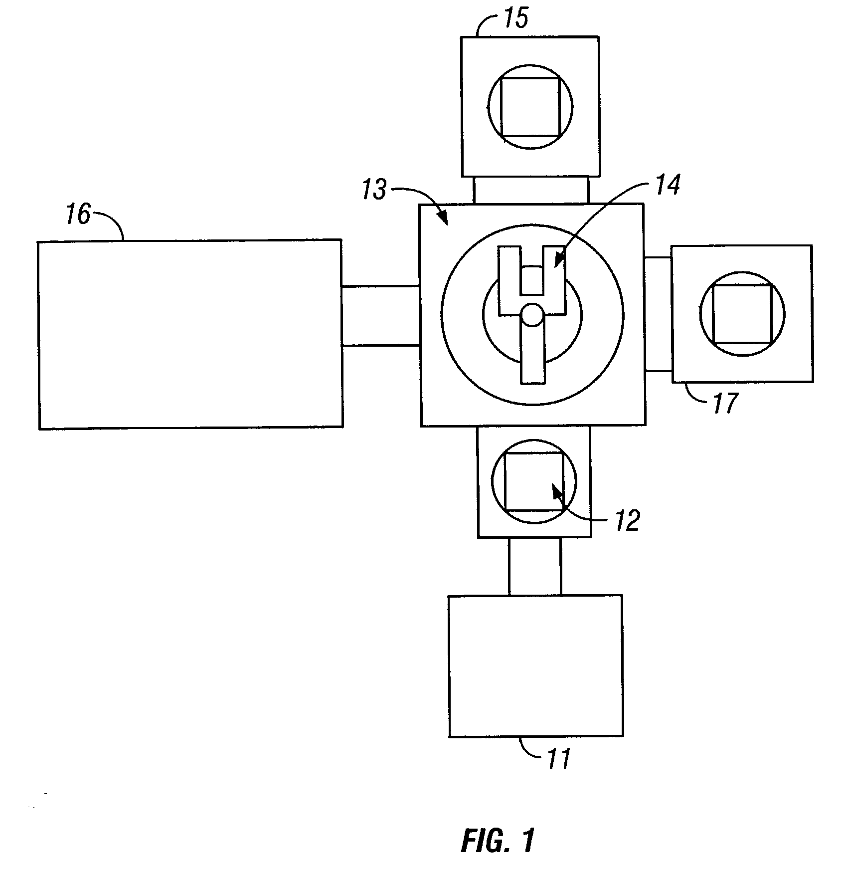
[0119]FIG. 1 shows the concept of a laser annealing apparatus used in this embodiment, which is of a multi-chamber type. Each substrate is input through a loader / unloader chamber 11, and then properly positioned in an alignment chamber 12. The substrate is then sequentially transferred to respective chambers via a transfer chamber 13 by means of a substrate transfer robot 14 that is provided in the transfer chamber 13, and processed in the respective chambers.
[0120]That is, a substrate is first input to a heat treatment chamber 15. After being subjected to a heat treatment, the substrate is subjected to laser annealing in a laser annealing chamber 16, cooled in a slow cooling chamber 17, and then moved to the loader / unloader chamber 11.
[0...
embodiment 2
[0162]This embodiment is directed to a case where a plurality of island-like patterned regions that are amorphous silicon films, on a glass substrate are converted by laser annealing into substantially single-crystalline silicon films, which are used as active layers of thin-film transistors.
[0163]As in the case of the first embodiment, the laser annealing apparatus of FIG. 1 is used in this embodiment.
[0164]An oscillator of type 3000-308 produced by Lambda Physic Corp. is used, which emits XeCl excimer laser light (wavelength: 308 nm; pulse width 26 ns). Naturally, other excimer lasers and other types of laser can be used as long as they are of a pulsed oscillation type.
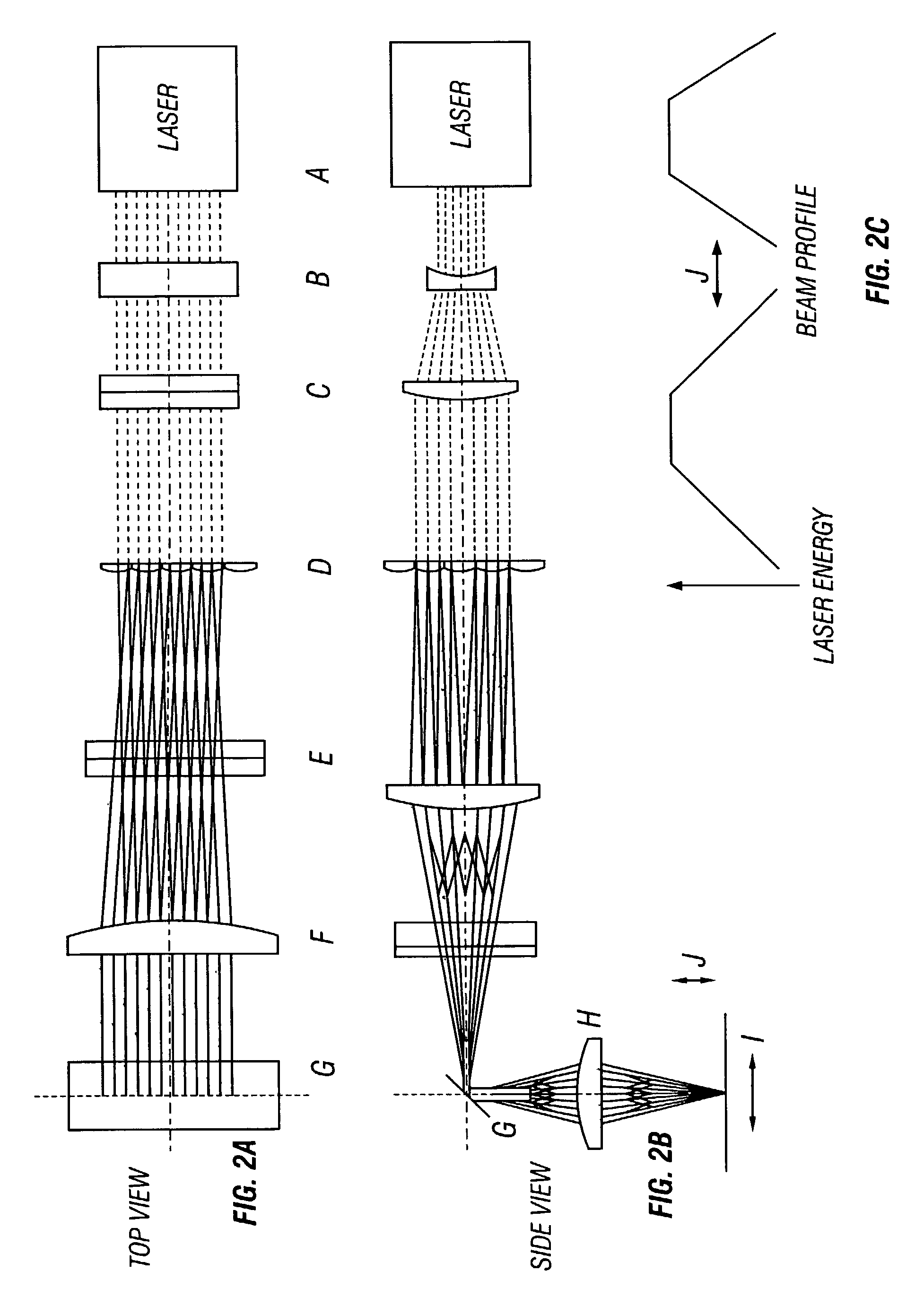
[0165]To transform the shape of an emitted laser beam, it is input to an optical system as shown in FIG. 3.
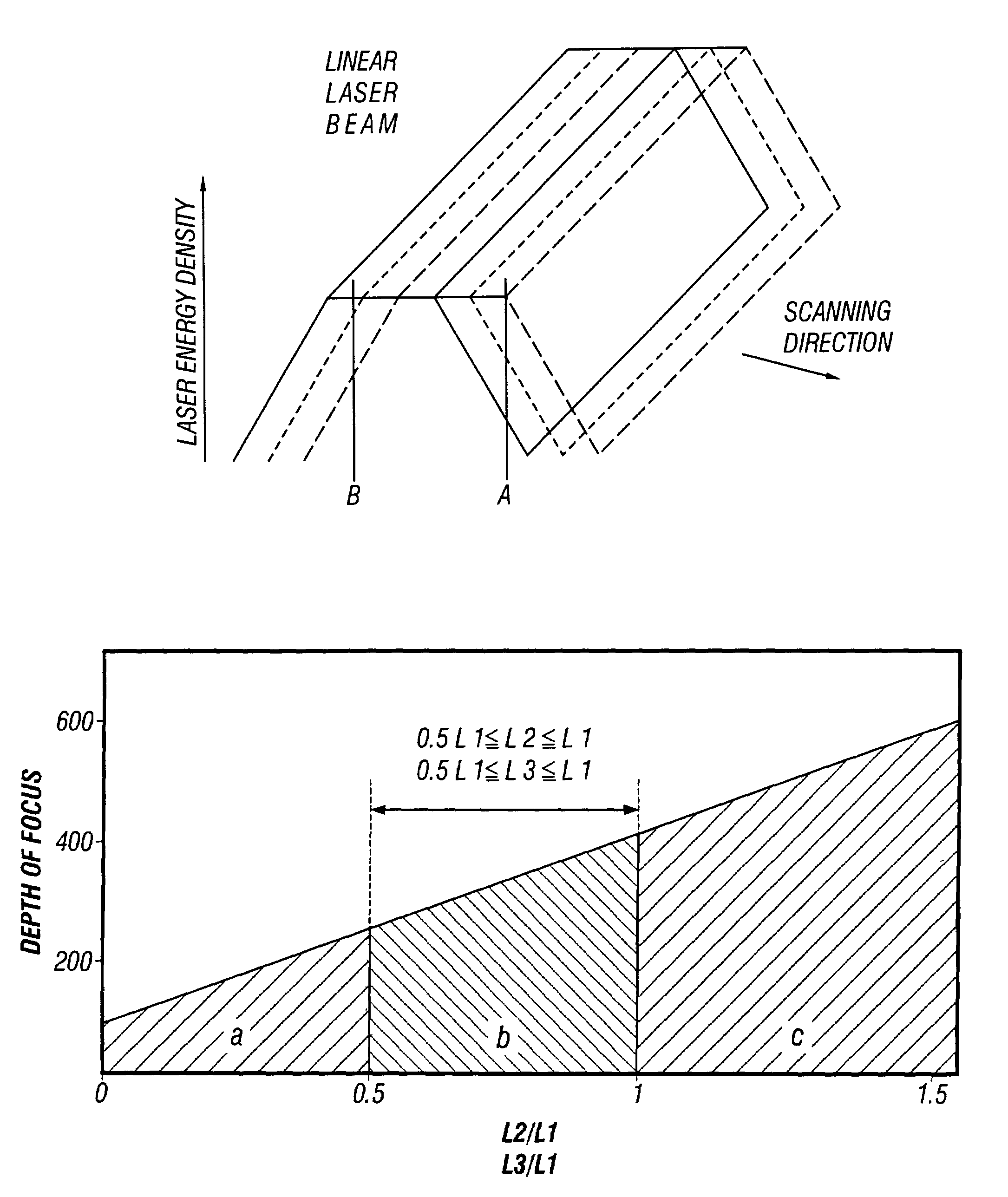
[0166]A laser beam, which assumes a rectangle of about 3×2 cm2 immediately before entering the optical system, is shaped into a long and narrow beam (i.e., linear beam) of 10 to 30 cm in length and 0.01 to 0.3 ...
embodiment 3
[0216]This embodiment uses the laser annealing apparatus of FIG. 1.
[0217]FIG. 9 shows an example of an optical system for laser annealing used in this embodiment.
[0218]The optical system of FIG. 9 is composed of the following components. An excimer laser beam generating means K (pulse laser beam generating means) generates an excimer laser beam. Beam expanders L and M expand the excimer laser beam. A compound-eye-like fly-eye lens N expands the laser beam in a sectional manner. A first cylindrical lens O converges the laser beam into a line shape. A second cylindrical lens P improves the uniformity of the linear laser beam in its longitudinal direction. A stage S is moved in direction T indicated by an arrow in FIG. 9 in a state that a substrate bearing an illumination object on its surface is placed thereon.
[0219]In FIG. 9, a path-folding mirror Q and a cylindrical lens R allow laser processing to be performed on the object placed on the stage S.
[0220]In this embodiment, the interv...
PUM
| Property | Measurement | Unit |
|---|---|---|
| temperature | aaaaa | aaaaa |
| temperature | aaaaa | aaaaa |
| depth of focus | aaaaa | aaaaa |
Abstract
Description
Claims
Application Information