Display substrate and manufacturing method thereof, display panel and display device

A technology for a display substrate and a manufacturing method, which is applied in the fields of display panels and display devices, display substrates and manufacturing methods thereof, and can solve the problems of poor display effects and reduced light extraction efficiency of display devices, etc.

Inactive Publication Date: 2017-06-27
BOE TECH GRP CO LTD
View PDF5 Cites 6 Cited by
  • Summary
  • Abstract
  • Description
  • Claims
  • Application Information

AI Technical Summary

Problems solved by technology

[0003] The collimated light emitted by the side-entry collimated backlight is transmitted from the side of the waveguide layer close to the backlight to the side of the waveguide layer away from the backlight. After applying an electrical signal to the electrode, the light enters the liquid crystal layer from the waveguide layer and then transmits The light to the side of the waveguide away from the backlight will decrease, so that the light output efficiency will gradually decrease in the direction of light transmission, and the side of the waveguide layer far away from the backlight may even appear close to the dark state, resulting in The display effect of the display device is poor

Method used


Image

  • Display substrate and manufacturing method thereof, display panel and display device
  • Display substrate and manufacturing method thereof, display panel and display device
  • Display substrate and manufacturing method thereof, display panel and display device

Examples


Embodiment Construction

[0042] In order to make the technical problems, technical solutions, and advantages to be solved by the embodiments of the present invention clearer, a detailed description will be given below with reference to the drawings and specific embodiments.

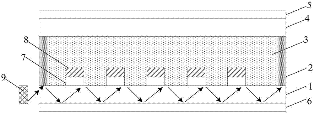
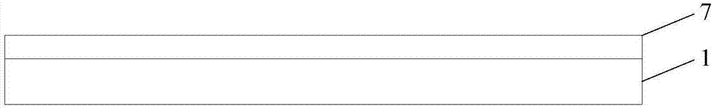
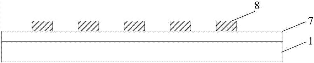
[0043] Such as figure 1 As shown, the existing display device includes a base substrate 1, 4 arranged in a pair of cells up and down, and a liquid crystal layer 3 located between the base substrates 1, 4, and a side of the base substrate 1 close to the liquid crystal layer 3 may be provided The waveguide layer, the refractive index of the waveguide layer is greater than the refractive index of the base substrate 1, or as figure 1 As shown, the base substrate 1 is directly used as the waveguide layer. The base substrate 1 is provided with a plurality of light-transmitting insulating patterns 7 arranged at intervals on the side close to the liquid crystal layer 3, and electrodes 8 are arranged on the light-transmitting insulating patter...


PUM


Abstract

The invention provides a display substrate and a manufacturing method thereof, a display panel and a display device and belongs to the technical field of display. The display substrate comprises a waveguide layer, a transparent insulation graph and electrodes; the transparent insulation graph is located on the waveguide layer, the refractive index of the transparent insulation graph is smaller than that of the waveguide layer, the transparent insulation graph includes multiple first parts and multiple second parts, the first parts and the second parts are different in thickness, the first parts and the second parts are identical in the extension direction and are arranged alternatively, the thickness of the part is greater than that of the second parts, and the thickness of the second parts is less than the wavelength / (2*the refractive index of the transparent insulation graph) of visible light; the electrodes are located on the first parts of the transparent insulation graph. By the arrangement, even luminous efficiency of the display device can be achieved, and display effect of the display device is improved.

Description

Technical field [0001] The present invention relates to the field of display technology, in particular to a display substrate and a manufacturing method thereof, a display panel and a display device. Background technique [0002] The prior art proposes a display device that includes a substrate arranged in a pair of cells up and down and a liquid crystal layer located between the substrates. A waveguide layer is arranged on the side of the lower substrate close to the liquid crystal layer, and the refractive index of the waveguide layer is greater than that of the lower substrate. The side of the waveguide layer close to the liquid crystal layer is provided with a plurality of light-transmitting insulating patterns arranged at intervals, and electrodes are arranged on the light-transmitting insulating patterns. The display device also includes an edge-type collimating backlight source, which emits The collimated light can enter the waveguide layer at a certain angle (greater than...

Claims


Application Information

Patent Timeline
Patent Type & Authority Applications(China)
IPC IPC(8): G02F1/13357G02F1/1333
Inventor 贺芳
Owner BOE TECH GRP CO LTD
Why Eureka
Try Eureka