Delay circuit and semiconductor device including same

a delay circuit and semiconductor technology, applied in the field of delay circuits, can solve problems such as unnecessarily delayed by the minimum delay tim

Active Publication Date: 2007-12-04
SAMSUNG ELECTRONICS CO LTD
View PDF21 Cites 14 Cited by
  • Summary
  • Abstract
  • Description
  • Claims
  • Application Information

AI Technical Summary

Benefits of technology

[0025]Selected embodiments of the present invention provide a delay circuit capable of maintaining a constant minimum delay time even where the number of delay blocks in the delay circuit is increased, and further capable of delaying an input signal only through selected delay blocks.
[0026]In addition, selected embodiments of the invention also provide a semiconductor device having a delay circuit which can maintain a constant minimum delay time even where the number of delay blocks is increased, and capable of delaying an input signal only through selected delay blocks.

Problems solved by technology

Thus, even where the delay circuit does not perform a delay operation, input signal “in” is still transmitted through all of the delay blocks and thus is unnecessarily delayed by the minimum delay time.

Method used


Image

  • Delay circuit and semiconductor device including same
  • Delay circuit and semiconductor device including same
  • Delay circuit and semiconductor device including same

Examples


Embodiment Construction

[0040]Exemplary embodiments of the invention are described below with reference to the corresponding drawings. These embodiments are presented as teaching examples. The actual scope of the invention is defined by the claims that follow.

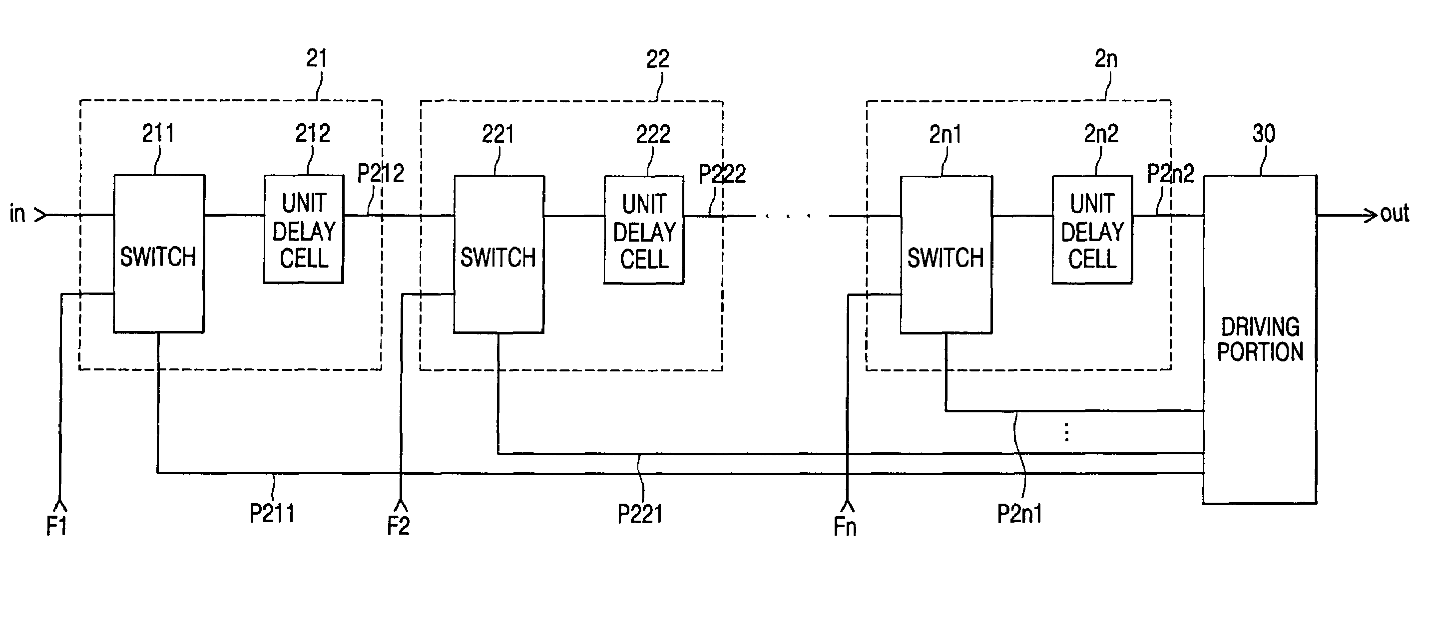
[0041]FIG. 4 is a block diagram illustrating a delay circuit according to one embodiment of the present invention. Referring to FIG. 4, the delay circuit includes a plurality of delay blocks 21 through 2n, which are serially connected to each other, and a driving portion 30 which is connected in parallel with delay blocks 21 through 2n. Delay blocks 21 through 2n include respective switches 211 through 2n1 and unit delay cells 212 through 2n2.

[0042]Delay blocks 21 through 2n also include first transmission paths P211 through P2n1, which are directly connected to driving portion 30, and second transmission paths P212 through P2n2, which are connected between successive delay blocks 21 through 2n and between delay block 2n and driving portion 30. Delay ...


PUM


Abstract

A delay circuit comprises a plurality of delay blocks connected in series, and a driving portion adapted to logically combine signals transmitted by the plurality of delay blocks to generate a delay circuit output signal. Each of the plurality of delay blocks delays an output signal from an immediately previous delay block and transmits a resulting delayed output signal to a next delay block when a delay operation is enabled based on a corresponding control signal. However, where the delay operation of a delay block is disabled based on the corresponding control signal, the delay block transmits the output signal of the immediately previous delay block to the driving portion.

Description

BACKGROUND OF THE INVENTION[0001]1. Field of the Invention[0002]The present invention relates generally to a delay circuit. More particularly, the invention relates to a delay circuit adapted to maintain a constant minimum delay time even where the number of delay blocks in the delay circuit increases, and to delay an input signal only through selected delay blocks.[0003]A claim of priority is made to Korean Patent Application No. 10-2005-0041322, filed May 17, 2005, the disclosure of which is hereby incorporated by reference in its entirety.[0004]2. Description of Related Art[0005]As the operating speed of semiconductor devices increases, the impact of small differences in a characteristic margin between signals in the semiconductor devices tends to increase accordingly. As a result, semiconductor devices often include a delay circuit having a plurality of delay blocks adapted to precisely control the timing of the signals within a signal path. The delay blocks are controlled by re...

Claims


Application Information

Patent Timeline
Patent Type & Authority Patents(United States)
IPC IPC(8): H03H11/26
CPCH03K5/133H03K2005/00058H03K5/14
Inventor CHO, YOUNG-CHULKIM, JOUNG-YEALKIM, SUNG-HOON
Owner SAMSUNG ELECTRONICS CO LTD
Why Eureka
Try Eureka