Method and apparatus for providing a rolling double reset timing for global storage in image sensors

a global storage and image sensor technology, applied in the field of semiconductor imagers, can solve the problems of low shutter efficiency (se), degrade image quality, increase the amount of dark current, etc., and achieve the effect of reducing the time between resets of storage nodes, reducing dark current and leakage charge generation, and improving the performance of global storage techniques

Active Publication Date: 2008-09-23
APTINA IMAGING CORP
View PDF5 Cites 16 Cited by
  • Summary
  • Abstract
  • Description
  • Claims
  • Application Information

AI Technical Summary

Benefits of technology

[0012]The present invention provides a new timing method and apparatus which improves the performance of global storage techniques. When a storage node is used for global storage, the timing method and apparatus helps to significantly reduce the dark current and the leakage charge generated in the storage node by using two rolling resets where one of the resets sweeps out the residue charge in the storage node prior to charge transfer from the storage node to the floating diffusion region. This rolling double reset minimizes the time between resets of the storage node and maintains a constant amount of time between resets of the storage node associated with different rows of the pixel array. This rolling double reset timing strategy reduces the dark current shading effects and shutter inefficiency effects. When the floating diffusion node is used for storing charge with a global shutter function, the timing method and apparatus also helps to significantly reduce the dark current generated in the floating diffusion node by using two rolling resets where a rolling shutter reset sweeps residue charge from the floating diffusion node prior to charge transfer from the photosensor and the storage node is effectively reset a second time when the charge is transferred from the floating diffusion node to the column select output line.

Problems solved by technology

Typically, one problem encountered when storage nodes are used with, for example, imagers including global storage, is the presence of an increased amount of dark current.
This may be caused by surface generation of the dark current or dark current resulting from process induced damage.
A second problem encountered with global storage pixels is leakage charge (or smear charge) which is the combination of optical and electrical crosstalk to the storage node resulting in a low shutter efficiency (SE).
The presence of dark current and leakage charge significantly degrades the image quality.

Method used


Image

  • Method and apparatus for providing a rolling double reset timing for global storage in image sensors
  • Method and apparatus for providing a rolling double reset timing for global storage in image sensors
  • Method and apparatus for providing a rolling double reset timing for global storage in image sensors

Examples


Embodiment Construction

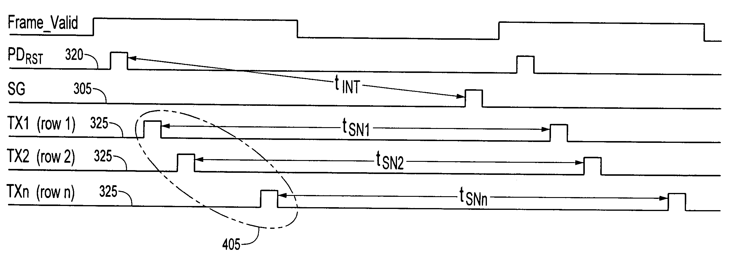
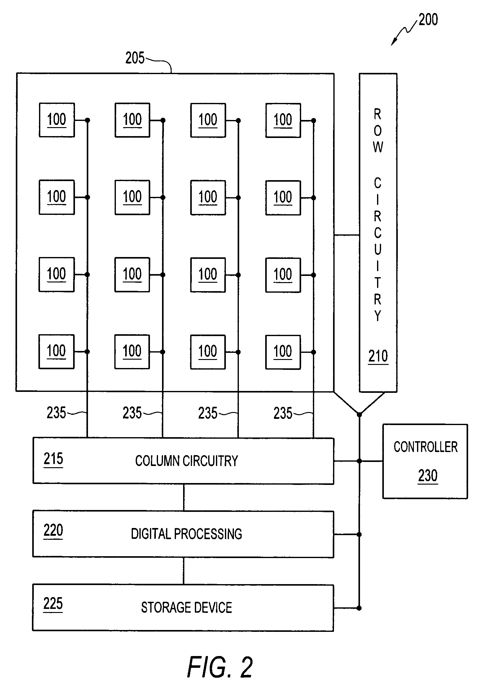
[0026]In the following detailed description, reference is made to the accompanying drawings, which are a part of the specification, and in which is shown by way of illustration, various embodiments whereby the invention may be practiced. These embodiments are described in sufficient detail to enable those skilled in the art to make and use the invention. It is to be understood that other embodiments may be utilized, and that structural, logical, and electrical changes, as well as changes in the materials used, may be made without departing from the spirit and scope of the present invention.

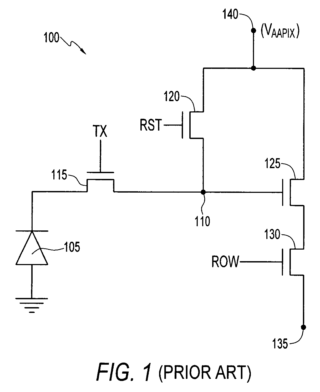
[0027]The term “substrate” is to be understood as referring to wafers or substrates including silicon, silicon-on-insulator (SOI) or silicon-on-sapphire (SOS), doped and undoped semiconductors, epitaxial layers of silicon supported by a base semiconductor foundation, and other semiconductor structures. Furthermore, when reference is made to a “substrate” in the following description, previous proc...


PUM


Abstract

An apparatus for and a method of operating an array of pixels of an image sensor, where each pixel includes at least a photosensor, an associated storage device and a floating diffusion region and the array of pixels is configured in a plurality of rows and columns. The photosensors associated with the pixels are reset and charges are accumulated in the photosensor. The accumulated charges are then globally transferred to storage devices associated with the pixels. A rolling double reset is used to reduce the deleterious effects on the accumulated charges stored in the storage devices. The accumulated charges stored in the storage devices are transferred to floating diffusion regions associated with the pixels and the charges residing in the floating diffusion region are read out. In a second embodiment the storage device is eliminated and the rolling double reset is used to reduce the deleterious effects on the accumulated charges stored in the floating diffusion region.

Description

FIELD OF INVENTION[0001]The present invention relates generally to semiconductor imagers. More specifically, the present invention relates to a novel timing methodology to improve the performance of global storage in imagers.BACKGROUND OF THE INVENTION[0002]An imager, for example, a CMOS imager includes a focal plane array of pixels; each pixel includes a photosensor, for example, a photogate, photoconductor or a photodiode overlying a substrate for producing a photo-generated charge in a doped region of the substrate. A readout circuit is provided for each pixel and includes at least a source follower transistor and a row select transistor for coupling the source follower transistor to a column output line. The pixel also typically has a floating diffusion region, connected to the gate of the source follower transistor. Charge generated by the photosensor is sent to the floating diffusion region. Imagers incorporating global storage include a transistor for transferring charge from...

Claims


Application Information

Patent Timeline
Patent Type & Authority Patents(United States)
IPC IPC(8): H01L27/00H04N5/217H04N9/64H04N5/359H04N5/361H04N5/3745
CPCH01L27/14609H04N5/359H04N5/3745H04N5/363H04N5/361H04N5/374H04N25/62H04N25/65H04N25/63H04N25/76H04N25/77
Inventor XU, CHENALTICE, PARKER
Owner APTINA IMAGING CORP
Why Eureka
Try Eureka