Sampling image signals generated by pixel circuits of an active pixel sensor (APS) image sensor in a sub-sampling mode

a technology of image signal and pixel circuit, which is applied in the field of sub-sampling of image signal generated by pixel circuit of an active pixel sensor (aps) image sensor, can solve the problems of significant image content loss and undesirable abrupt transition

Inactive Publication Date: 2007-12-04
AVAGO TECH WIRELESS IP SINGAPORE PTE
View PDF11 Cites 38 Cited by
  • Summary
  • Abstract
  • Description
  • Claims
  • Application Information

AI Technical Summary

Problems solved by technology

Unfortunately, a drawback of conventional sub-sampling methods is that significant image content is lost by not sampling the skipped pixels.
The missing information can result in undesirable abrupt transitions at the boundary between sampled and skipped pixels in the captured image.

Method used


Image

  • Sampling image signals generated by pixel circuits of an active pixel sensor (APS) image sensor in a sub-sampling mode
  • Sampling image signals generated by pixel circuits of an active pixel sensor (APS) image sensor in a sub-sampling mode
  • Sampling image signals generated by pixel circuits of an active pixel sensor (APS) image sensor in a sub-sampling mode

Examples


Embodiment Construction

[0014]In the following detailed description of the preferred embodiments, reference is made to the accompanying drawings, which form a part hereof, and in which is shown by way of illustration specific embodiments in which the invention may be practiced. It is to be understood that other embodiments may be utilized and structural or logical changes may be made without departing from the scope of the present invention. The following detailed description, therefore, is not to be taken in a limiting sense, and the scope of the present invention is defined by the appended claims.

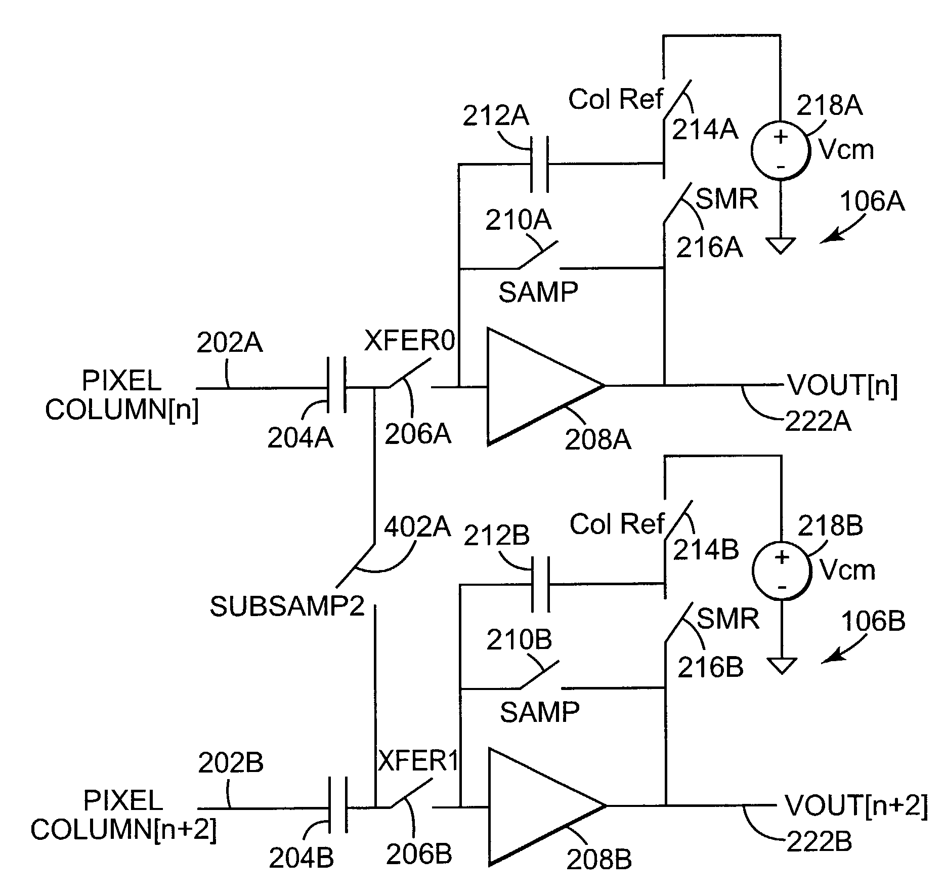
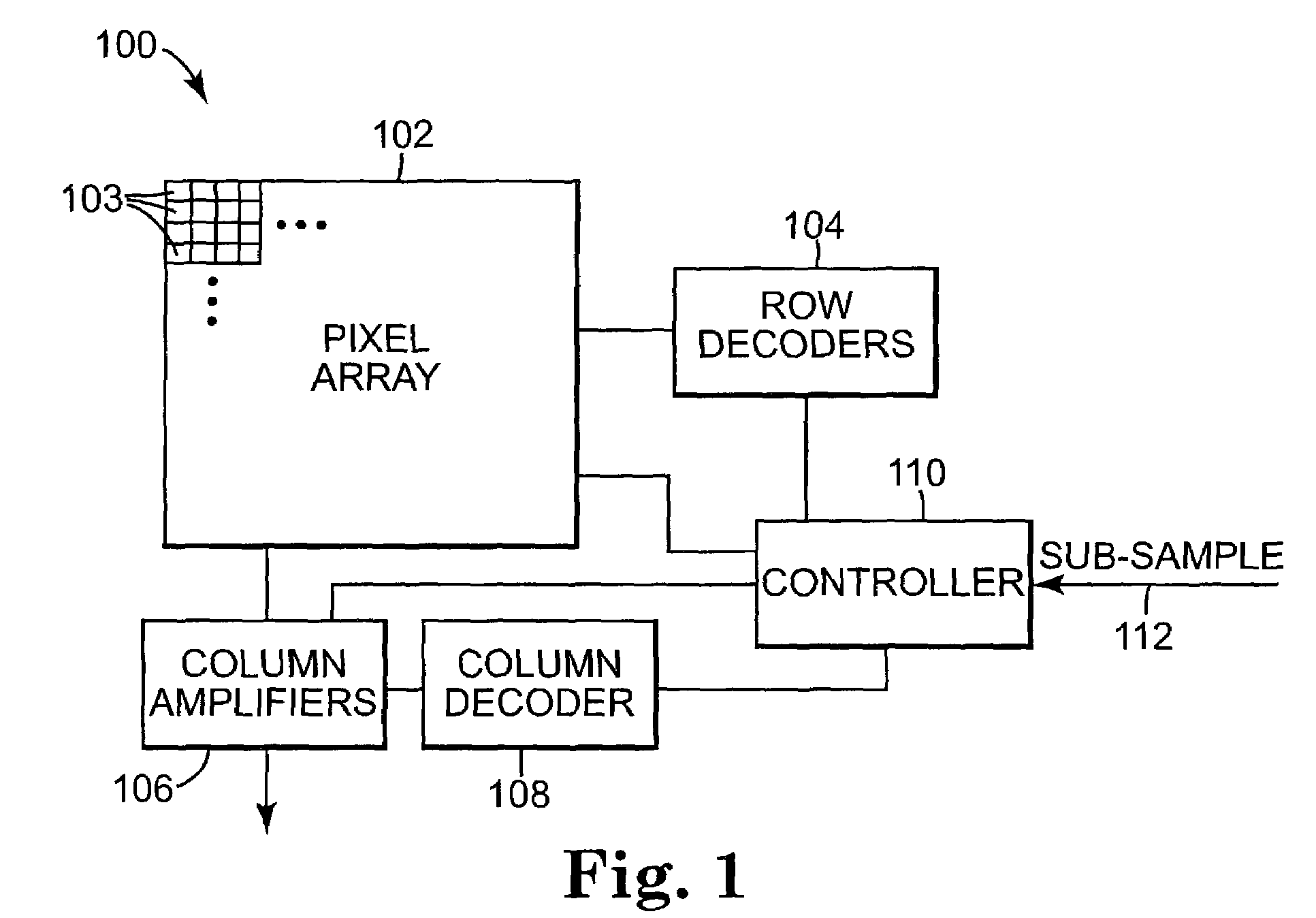
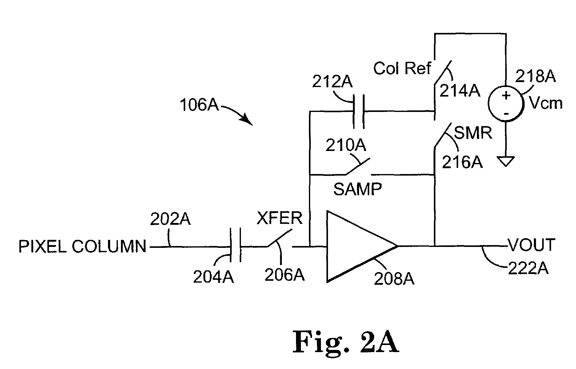
[0015]FIG. 1 is a block diagram illustrating major components of an active pixel sensor (APS) image sensor 100 according to one embodiment of the present invention. Sensor 100 includes pixel array 102, row decoders 104, column amplifiers 106, column decoder 108, and controller 110. Pixel array 102 includes a plurality of pixel circuits (pixels) 103, with each pixel circuit 103 providing one pixel of image inform...


PUM


Abstract

A method of sampling image signals generated by pixel circuits of an active pixel sensor (APS) image sensor. The APS image sensor supports a normal mode of operation and a sub-sampling mode of operation. The method includes providing a plurality of column amplifiers. A row of pixels circuits to sample is selected. Image signals from each pixel circuit in the selected row are routed to a different one of the plurality of column amplifiers when the APS image sensor is in the normal mode of operation. Image signals from a plurality of the pixel circuits in the selected row are routed to one of the plurality of column amplifiers when the APS image sensor is in the sub-sampling mode of operation.

Description

THE FIELD OF THE INVENTION[0001]The present invention generally relates to active pixel sensor (APS) image sensors, and more particularly to the sampling of image signals generated by pixel circuits of an APS image sensor in a sub-sampling mode.BACKGROUND OF THE INVENTION[0002]One type of prior art image sensor is a charge-coupled device (CCD) image sensor. CCD image sensors typically include a very closely packed array of polysilicon electrodes that are formed on the surface of the CCD imaging chip. Conceptually, a CCD is a two-dimensional array of Metal Oxide Semiconductor (MOS) capacitors that collect and transfer photon-generated charge. CCD image sensors typically include multiple shift registers to transfer charge from the CCD array to amplifiers.[0003]Another type of prior art image sensor is an active pixel sensor (APS) image sensor. APS image sensors are typically fabricated using Complimentary Metal Oxide Silicon (CMOS) processing technology, and are also typically referre...

Claims


Application Information

Patent Timeline
Patent Type & Authority Patents(United States)
IPC IPC(8): H04N3/14H01L27/146H04N5/343H04N5/374H04N5/378
CPCH04N5/335H04N25/00
Inventor MENTZER, RAY A.BORG, MATTHEW M.
Owner AVAGO TECH WIRELESS IP SINGAPORE PTE
Why Eureka
Try Eureka