

Data input buffer in semiconductor device
a data input buffer and semiconductor device technology, applied in the field of input buffers, can solve the problems of static input buffers that are not suitable for use in semiconductor devices, input buffers with problems controlling operation speed, and static input buffers that are sensitive to noise, etc., and achieve high operation speed and reduce current consumption
- Summary
- Abstract
- Description
- Claims
- Application Information
AI Technical Summary
Benefits of technology
Problems solved by technology
Method used
Image



Examples
Embodiment Construction
[0024]Hereinafter, an input buffer for use in a semiconductor device in accordance with the present invention will be described in detail referring to the accompanying drawings.
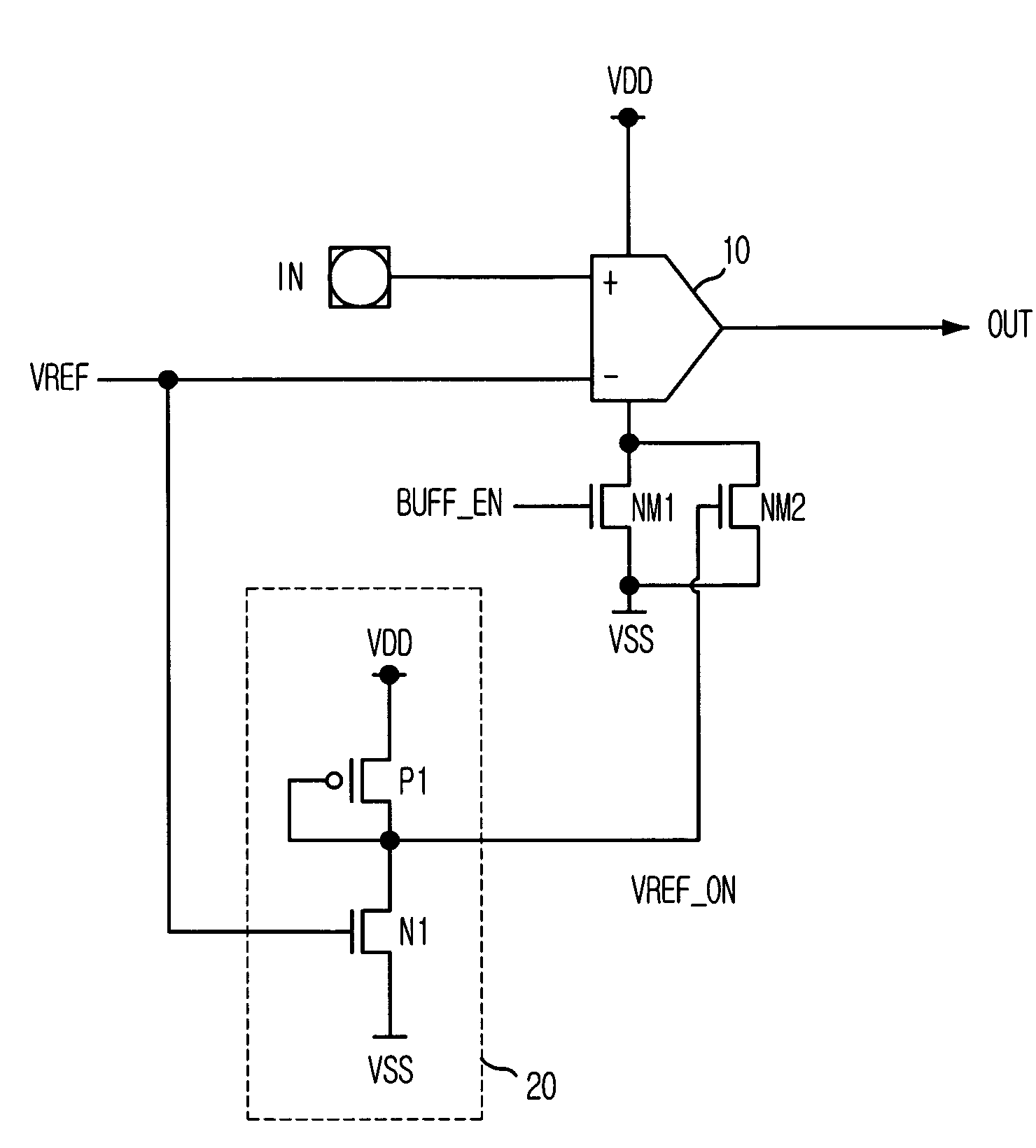
[0025]FIG. 3 is a schematic circuit diagram depicting an input buffer in accordance with a preferred embodiment of the present invention.
[0026]As shown, the input buffer includes a first bias NMOS transistor NM1 controlled by a buffer enable signal BUFF_EN, a comparator 10 for sensing a logic level of an input data IN by comparing with a voltage level of the input data IN with that of a reference voltage VREF, a reference voltage detector 20 for detecting a voltage level of the reference voltage VREF, and a second bias NMOS transistor NM2 controlled by an output signal VREF_ON from the reference voltage detector 20 and parallel connected to the first bias NMOS transistor NM1.
[0027]Herein, the reference voltage detector 20 is provided with a first NMOS transistor N1 and a first PMOS transistor P1. The first NM...
PUM
 Abstract
Description
Claims
Application Information