
OLED display with aging compensation

Inactive Publication Date: 2008-01-22
GLOBAL OLED TECH
View PDF42 Cites 295 Cited by
  • Summary
  • Abstract
  • Description
  • Claims
  • Application Information

AI Technical Summary

Benefits of technology

[0017]The advantages of this invention are an OLED display that compensates for the aging of the organic materials in

Problems solved by technology

However, as the display is used, the organic materials in the display age and become less efficient at emitting light.
This reduces the lifetime of the display.
The differing organic materials may age at different rates, causing differential color aging and a display whose white point varies as the display is used.
Unfortunately, over time the characteristics of any display device can change.
For example, when charge is stored at a pixel, the charge decays, affecting the brightness or color of the pixel.
Alternatively, as time passes and a display device is used, the nature of the pixel can change: transistors become less efficient or responsive, impurities creep into display elements causing them to decrease in brightness or change in color, etc.
This technique requires the measurement and accumulation of drive current applied to each pixel, requiring a stored memory that must be continuously updated as the display is used, requiring complex and extensive circuitry.
This design requires the use of an integrated, calibrated current source and A / D converter, greatly increasing the complexity of the circuit design.
This design requires the use of a calculation unit responsive to each signal sent to each pixel to record usage, greatly increasing the complexity of the circuit design.
Such circuits are difficult to design and expensive to build.
Moreover, the measurement techniques are iterative and therefore slow and rely upon a voltage source drive while OLED displays are preferably controlled using constant current sources.

Method used


Image

  • OLED display with aging compensation
  • OLED display with aging compensation
  • OLED display with aging compensation

Examples


Embodiment Construction

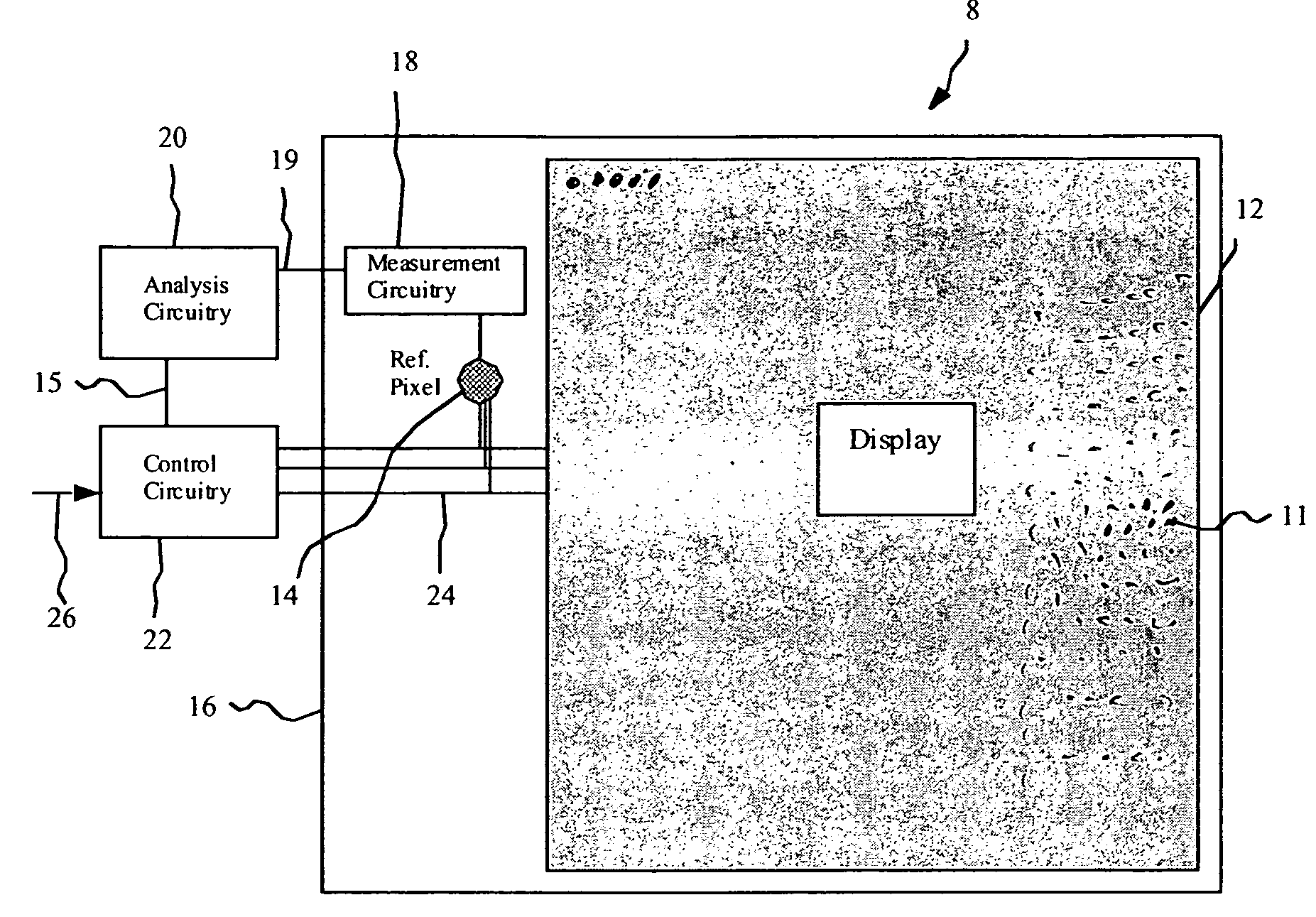
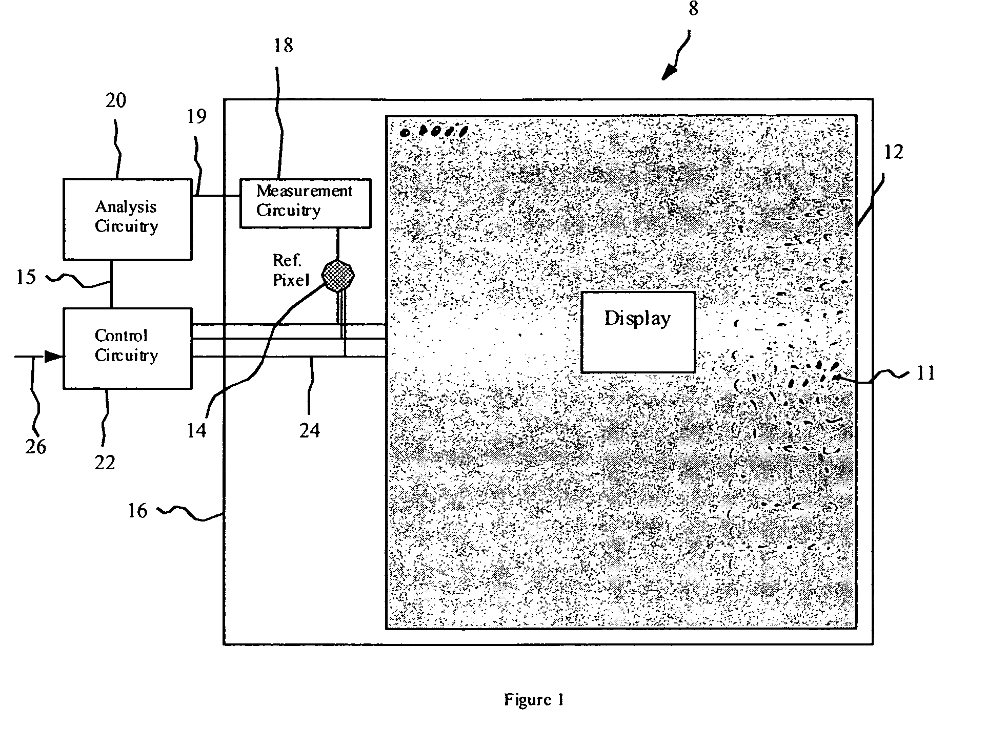
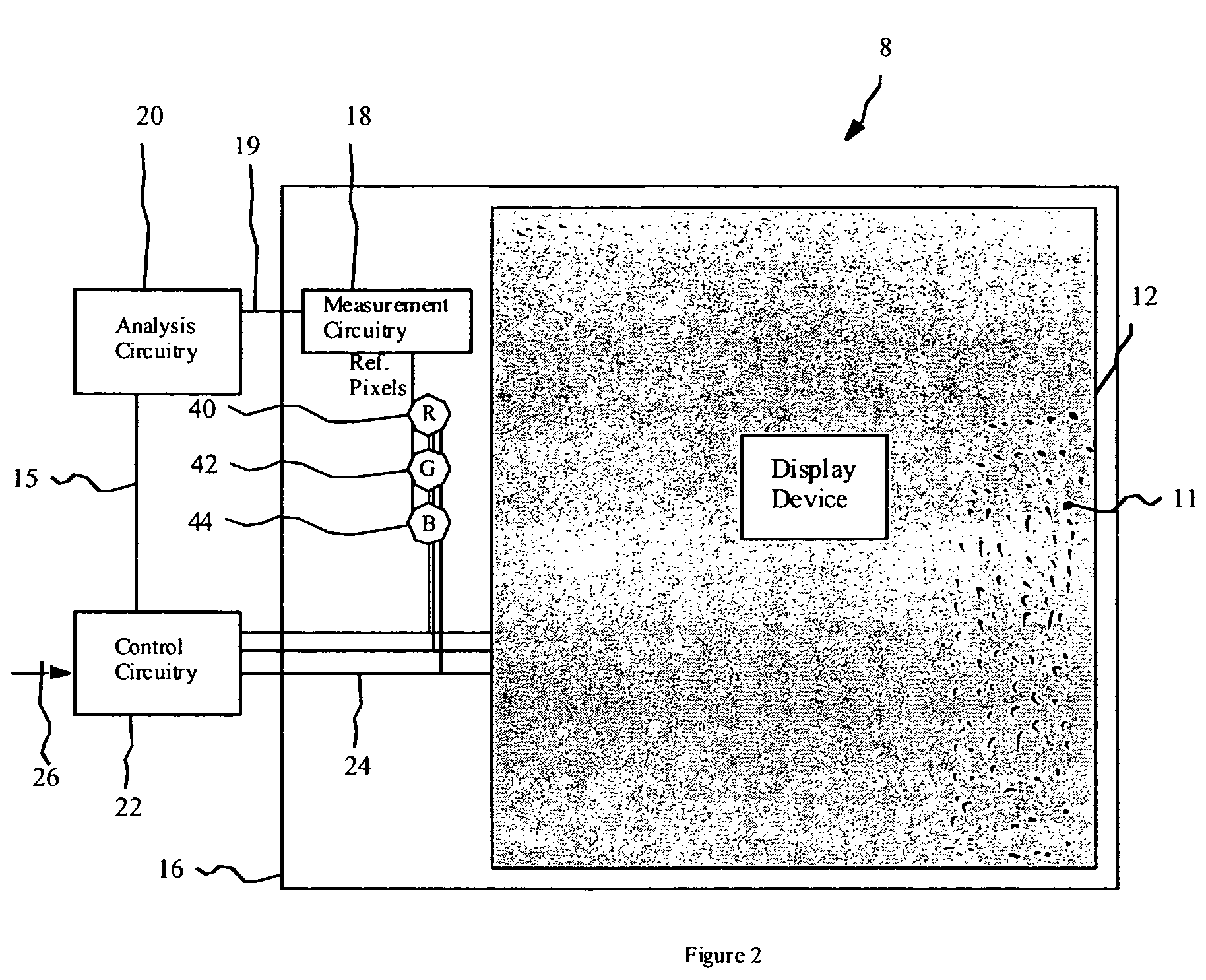
[0025]The present invention describes a display that overcomes the problems in the prior art through the use of reference pixels to enable the measurement of pixel performance and a feedback mechanism responsive to the measured pixel performance to modify the operating characteristics of the display device. These operational changes improve the performance of the display device.

[0026]The solid-state image display device with a reference pixel is composed of a standard, solid-state display device having an array or collection of pixels supplemented by an additional reference pixel or pixels that have the same performance attributes as the pixels in the display device. According to a preferred embodiment of the invention, the pixels are OLEDs having a local charge storage mechanism and a transistor drive circuit activated by the stored charge for applying power to each pixel. The reference pixels can be instrumented with a voltage measurement circuit that is connected to an analysis c...


PUM


Abstract

An organic light-emitting diode (OLED) display having addressable pixels on a substrate, the pixels having performance attributes, and a control circuit for controlling the pixels of the display device, includes one or more OLED pixels; an OLED reference pixel located on a substrate and connected to the control circuit, the OLED reference pixel having the same performance attributes as the one or more OLED pixels, the OLED reference pixel having a voltage sensing circuit including a transistor connected to one of the terminals of the OLED reference pixel for sensing the voltage across the OLED reference pixel to produce a voltage signal representing the voltage across the OLED reference pixel; a measurement circuit connected to the voltage signal to produce an output signal representative of the performance attributes of the OLED reference pixel; an analysis circuit connected to the measurement circuit to receive the output signal, compare the performance attributes with predetermined performance attributes, and produce a feedback signal in response thereto; and the control circuit being responsive to the feedback signal to compensate for changes in the output of the OLED pixels.

Description

[0001]This is a continuation-in-part of application U.S. Ser. No. 09 / 577,241 filed May 24, 2000 now abandoned.FIELD OF THE INVENTION[0002]The present invention relates to solid-state OLED flat-panel displays and more particularly to such displays having means to compensate for the aging of the organic light-emitting display.BACKGROUND OF THE INVENTION[0003]Solid-state organic light-emitting diode (OLED) displays are of great interest as a superior flat-panel display technology. These displays utilize current passing through thin films of organic material to generate light. The color of light emitted and the efficiency of the energy conversion from current to light are determined by the composition of the organic thin-film material. Different organic materials emit different colors of light. However, as the display is used, the organic materials in the display age and become less efficient at emitting light. This reduces the lifetime of the display. The differing organic materials ma...

Claims


Application Information

Patent Timeline
IPC IPC(8): G09G3/32G09G3/20G09G3/30H01L51/50
CPCG09G3/3225G09G3/3258G09G2300/0465G09G2320/029G09G2320/043G09G2320/0626G09G2360/14G09G2360/145
Inventor COK, RONALD S.NIERTIT, THOMASARNOLD, ANDREW D.
Owner GLOBAL OLED TECH
Learn More