Recess gate-type semiconductor device and method of manufacturing the same

a semiconductor device and gate-type technology, applied in the field of semiconductor devices, can solve the problems of increasing the off-current that is present in the transistor, deteriorating the refresh characteristics of a semiconductor device such as a memory device, etc., and achieves the effects of reducing junction leakage current, good refresh characteristics, and good refresh characteristics

Inactive Publication Date: 2008-01-29
SAMSUNG ELECTRONICS CO LTD
View PDF11 Cites 7 Cited by
  • Summary
  • Abstract
  • Description
  • Claims
  • Application Information

AI Technical Summary

Benefits of technology

[0015]According to some embodiments of the invention, a recess gate-type semiconductor device provides good refresh characteristics resulting from a decrease of a junction leakage current. According to other embodiments of the invention, a method of manufacturing a recess gate-type semiconductor device results in a device that provides good refresh characteristics resulting from a decrease of a junction leakage current.

Problems solved by technology

In addition, the decrease in the channel length results in an increased short channel effect, thus increasing an off-current that is present in the transistors.
As a result, the refresh characteristics of a semiconductor device such as a memory device may deteriorate.

Method used


Image

  • Recess gate-type semiconductor device and method of manufacturing the same
  • Recess gate-type semiconductor device and method of manufacturing the same
  • Recess gate-type semiconductor device and method of manufacturing the same

Examples


Embodiment Construction

[0032]The invention is described more fully below with reference to the accompanying drawings, in which exemplary embodiments of the invention are shown. The invention may, however, be embodied in many different forms and should not be construed as being limited to the embodiments set forth herein; rather, these embodiments are provided so that this disclosure will be thorough and complete, and will fully convey the concept of the invention to those skilled in the art. In the drawings, the thicknesses of layers and regions may be exaggerated for clarity.

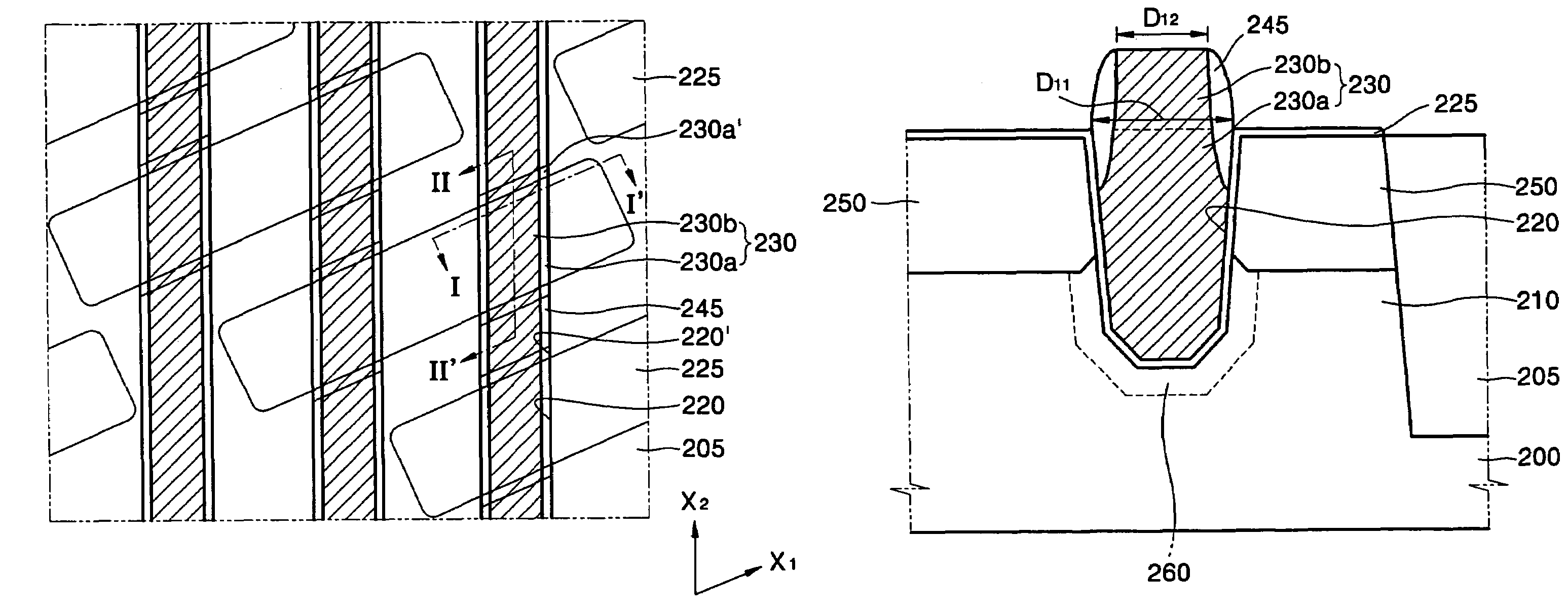
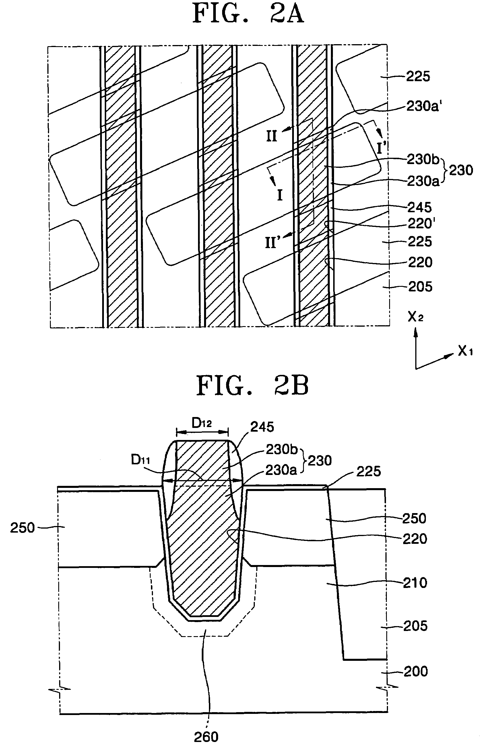
[0033]FIG. 2A is a plan diagram illustrating a recess gate-type semiconductor device according to some embodiments of the invention. FIG. 2B is a sectional diagram, taken along the line I-I′ of FIG. 2A, which further illustrates the device of FIG. 2A. FIG. 2C is a sectional diagram, taken along the line II-II′ of FIG. 2A, which further illustrates the device of FIG. 2A.

[0034]Referring to FIGS. 2A through 2C, a semiconductor device in...


PUM


Abstract

A recess gate-type semiconductor device includes a gate electrode having a recessed portion at least partially covering a recess trench in an active region, and source / drain regions disposed in the active region that are separated by the gate electrode. The recess trench is separated from sidewalls of a device isolation region in a first direction and contacts sidewalls of the device isolation region in a second direction. The width of the recess trench of the active region in the second direction may be greater than the width of the source / drain regions in the second direction, and the recessed portion of the gate electrode may have tabs protruding in the first direction at its corners. Therefore, the semiconductor device has excellent junction leakage current and excellent refresh characteristics.

Description

CROSS-REFERENCE TO RELATED APPLICATIONS[0001]This application claims priority from Korean Patent Application No. 10-2004-0073371, filed on 14 Sep. 2004, and Korean Patent Application No. 10-2005-0032293, filed on 19 Apr. 2005, the contents of which are hereby incorporated by reference in their entirety for all purposes.BACKGROUND[0002]1. Field of the Invention[0003]This disclosure relates to semiconductor devices and more particularly, to a recess gate-type semiconductor device and a method of manufacturing the same.[0004]2. Description of the Related Art[0005]As semiconductor devices become highly integrated, design rules for semiconductor device components decrease. In particular, for semiconductor devices having many transistors, a gate length, which is a standard of the design rule, decreases. Thus, a channel length of the transistor must also decrease. In addition, the decrease in the channel length results in an increased short channel effect, thus increasing an off-current th...

Claims


Application Information

Patent Timeline
Patent Type & Authority Patents(United States)
IPC IPC(8): H01L27/108H01L29/94
CPCH01L29/0692H01L29/4236H01L29/42376
Inventor PARK, WON-MOPAIK, JAE-CHOELSONG, DU-HEONKIM, DONG-HYUNLEE, CHANG-SUB
Owner SAMSUNG ELECTRONICS CO LTD
Why Eureka
Try Eureka