Semiconductor memory device having dummy word line

a memory device and memory line technology, applied in semiconductor devices, digital storage, instruments, etc., can solve the problems of reducing the processing efficiency of the system, increasing the power consumption of refreshing, and affecting the performance of the device, so as to improve the refresh characteristics and manufacturing yield of the semiconductor memory device, the effect of improving the refresh tim

Inactive Publication Date: 2005-10-06
RENESAS ELECTRONICS CORP
View PDF10 Cites 3 Cited by
  • Summary
  • Abstract
  • Description
  • Claims
  • Application Information

AI Technical Summary

Benefits of technology

[0123] For example, as shown in FIG. 13, isolated cell plate 130# may be arranged for each memory cell row in the layout according to the first embodiment shown in FIG. 2. In this case, each isolated cell plate 130# can be shared by a plurality of (two in FIG. 13) twin-cell units belonging to the same memory cell column. For this arrangement, however, it is essential that the voltages on the storage nodes storing the complementary data in each twin-cell unit vary within a similar range owing to the capacitive coupling. These voltage variations are caused by suppressing the capacitance of each isolated cell plate. Therefore, the effect of the invention is remarkably achieved by isolating the cell plate for each twin- cell unit.
[0125] A fourth embodiment will now be described in connection with a structure of a twin-cell unit further improving refresh characteristics.
[0126]FIG. 14 schematically shows a structure of a memory array portion of a semiconductor memory device according to the fourth

Problems solved by technology

In the DRAM cell, since a capacitor is used as a data record medium, the stored data may disappear due to a leak current.
Therefore, the shorter refresh interval lowers the processing efficiency of the system.
Further, a power consumption for the refreshing increases.
In this case, the storage capacity decreases to half the capacity of the single-cell DRAM of the one-bit / one-cell type, and it becomes difficult to achieve a twin-cell DRAM of a large storage capacity.

Method used


Image

  • Semiconductor memory device having dummy word line
  • Semiconductor memory device having dummy word line
  • Semiconductor memory device having dummy word line

Examples


first embodiment

[0045] First Embodiment

[0046] A memory cell structure of a twin-cell DRAM according to an embodiment of the invention, which has improved refresh characteristics, will now be described with reference to the drawings.

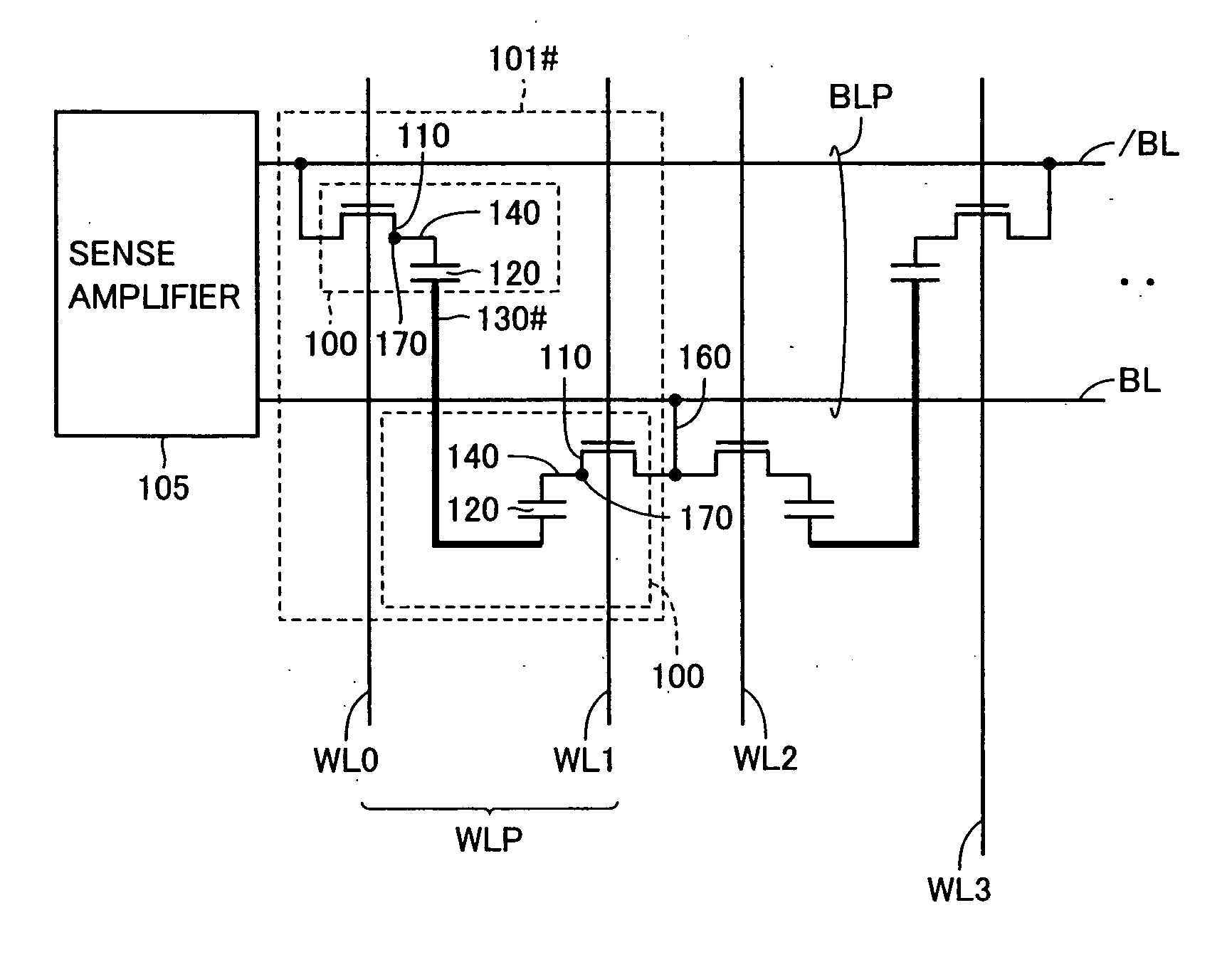
[0047] Referring to FIG. 1, a twin-cell unit 101# according to a first embodiment is formed of two DRAM cells 100, which are connected to paired complementary bit lines BL and / BL, respectively, similarly to a conventional twin-cell unit 101 shown in FIG. 17. Each DRAM cell 100 includes an access transistor 110 and a capacitor 120, as is already described with reference to FIG. 17. Access transistors 110 of two DRAM cells 100 forming twin-cell unit 101# have gates connected to two word lines (e.g., word lines WL0 and WL1) forming a word line pair WLP, respectively.

[0048] In the twin-cell DRAM according to the first embodiment, a cell plate structure is formed of isolated cell plates 130#, which are divided from each other and correspond to twin-cell units 101#, respect...

second embodiment

[0080] Second Embodiment

[0081] In the twin-cell DRAM, it is important to arrange the DRAM cells at a high density for reducing a layout area, as already described. Therefore, second and third embodiments will now be described in connection with layouts for efficiently arranging the twin-cell units, which have been described in connection with the first embodiment.

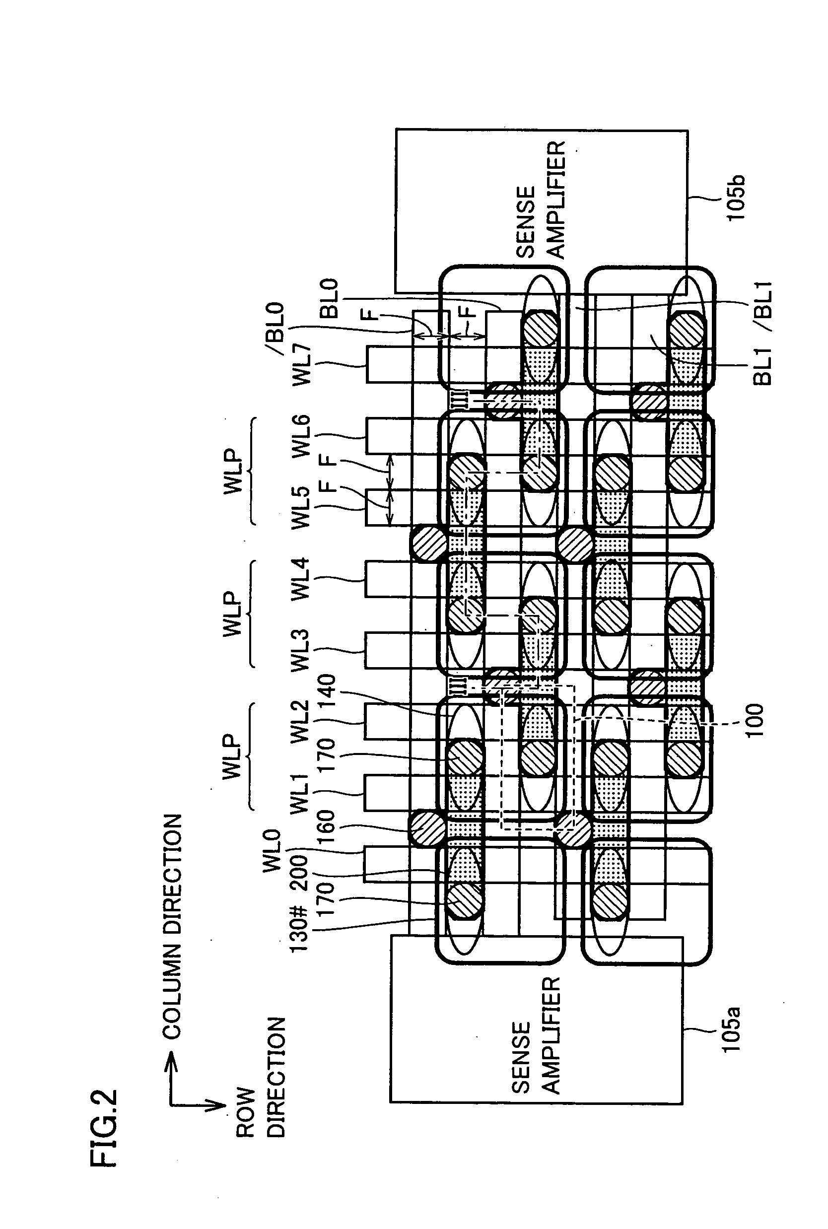
[0082] Referring to FIG. 5, which shows a structure according to the second embodiment, two DRAM cells 100 forming the same twin-cell unit 101# are selected by common word line WL. Structures of the second embodiment other than the above are substantially the same as those of the first embodiment. Therefore, corresponding portions bear the same reference numbers, and description thereof is not repeated.

[0083]FIG. 6 schematically shows a layout of a memory array portion in the semiconductor memory device according to the second embodiment.

[0084] In FIG. 6, word lines WL0-WL5 extend in the row direction. Bit lines BL0 and ...

third embodiment

[0092] Third Embodiment

[0093]FIG. 7 schematically shows a structure of a memory array portion in a semiconductor memory device according to a third embodiment of the invention.

[0094] Referring to FIG. 7, a structure according to the third embodiment includes dummy word lines DWL formed along word lines WL, in addition to the structures of the second embodiment shown in FIG. 5. Structures other than the above are substantially the same as those according to the second embodiment shown in FIG. 5. Corresponding portions bear the same reference numbers, and description thereof is not repeated.

[0095]FIG. 8 schematically shows a layout of a memory array portion in the semiconductor memory device according to the third embodiment.

[0096] Referring to FIG. 8, the layout according to the third embodiment differs from the layout according to the second embodiment shown in FIG. 6 in the following points. Dummy word line DWL is arranged between storage node contacts 170, which are formed in f...


PUM


Abstract

Each cell unit has a cell plate electrically isolated from the cell plates in the other cell units.

Description

TITLE OF THE INVENTION [0001] Semiconductor Memory Device Having Twin-Cell Units BACKGROUND OF THE INVENTION [0002] 1. Field of the Invention [0003] The present invention relates to a semiconductor memory device, and particularly to a twin-cell DRAM (Dynamic Random Access Memory) storing one bit of data by two memory cells. More particularly, the invention relates to a memory cell structure of a DRAM, which is formed of twin-cell structures and has improved refresh characteristics. [0004] 2. Description of the Background Art [0005] For example, Japanese Patent Laying-Open No. 7-130172, which will be referred to as a “prior art 1” hereinafter, has disclosed a twin-cell DRAM storing one bit of data by two memory cells for suppressing lowering of an operation margin such as lowering of a read voltage, which may occur in memory cells having a reduced layout area. [0006] In the prior art 1, a layout of memory cells is similar to that of general DRAM cells storing one bit of data by one c...

Claims


Application Information

Patent Timeline
Patent Type & Authority Applications(United States)
IPC IPC(8): G11C7/18H01L27/108G11C11/401G11C11/404G11C11/405G11C11/4097H01L21/8242H01L27/02
CPCG11C7/18G11C11/405G11C11/4097G11C2211/4013H01L27/10814H01L27/10882H01L27/0207H10B12/315H10B12/48H10B12/00
Inventor TSUKIKAWA, YASUHIKOITO, TAKASHI
Owner RENESAS ELECTRONICS CORP
Why Eureka
Try Eureka