Semiconductor device and method for manufacturing the same

Active Publication Date: 2010-04-29
RENESAS ELECTRONICS CORP
View PDF9 Cites 5 Cited by
  • Summary
  • Abstract
  • Description
  • Claims
  • Application Information

AI Technical Summary

Benefits of technology

[0016]According to the present invention, it is possible to suppress an increment in capacitance between interconnects

Problems solved by technology

There are various kinds of low dielectric constant layers, but low dielectric constant layers are commonly poor in adhesion or mechanical strength.
Therefore, there is a problem in that when a trench is formed in a low dielectric constant layer, an altered (degraded) layer is formed on a sidewall of the trench (concave portion) during an etching process or a resist ashing process, and thus an effective k val

Method used


Image

  • Semiconductor device and method for manufacturing the same
  • Semiconductor device and method for manufacturing the same
  • Semiconductor device and method for manufacturing the same

Examples


first exemplary embodiment

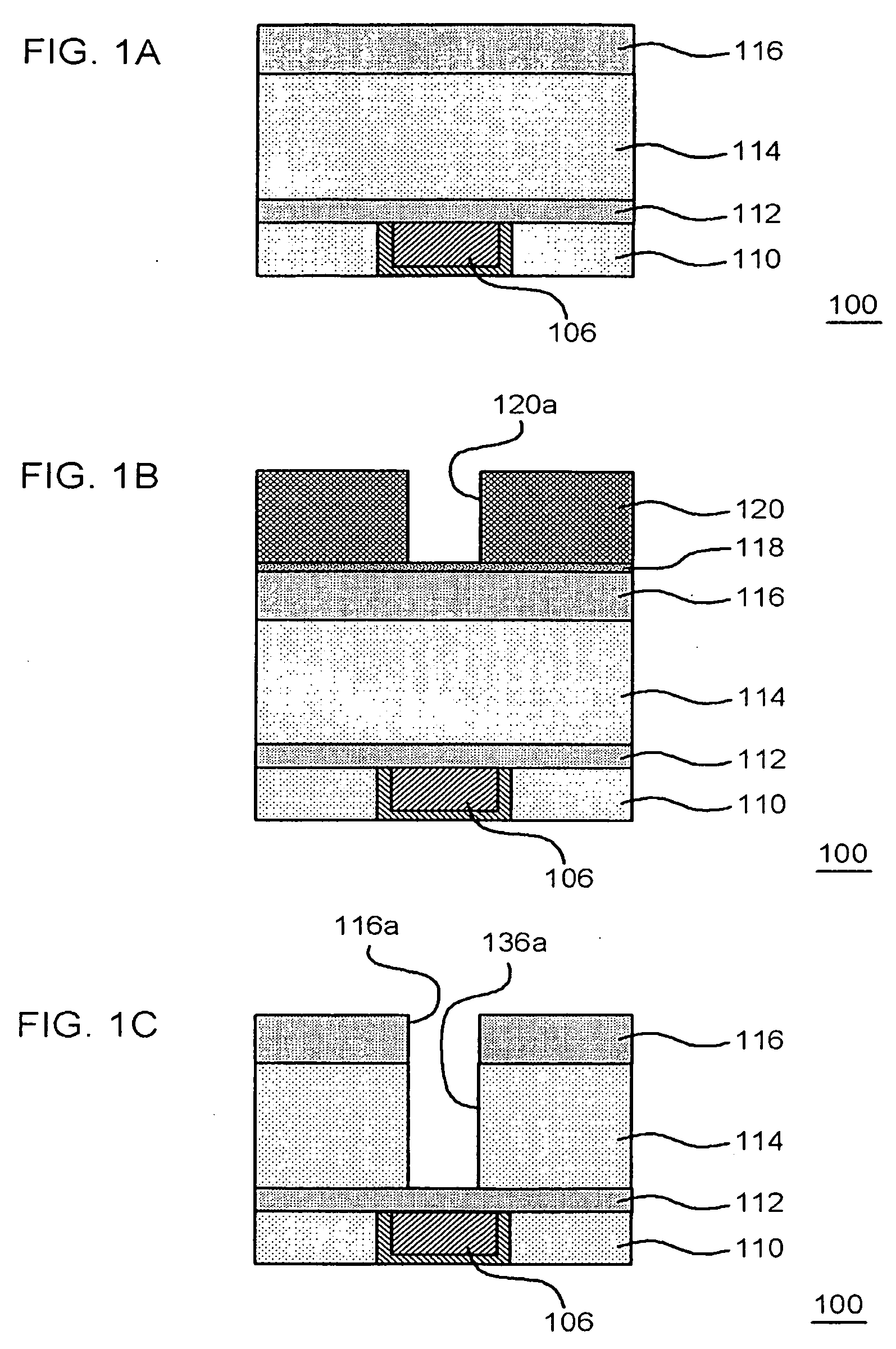
[0029]FIGS. 1A to 4 are cross-sectional views illustrating a procedure of manufacturing a semiconductor device according to the exemplary embodiment of the present invention.

[0030]In the exemplary embodiment of the present invention, a procedure for forming a dual damascene trench (including both a wiring trench and a via trench) in a low dielectric constant layer by “via first method” will be described.

[0031]A semiconductor device 100 has a structure that an insulating interlayer 110 is formed on a substrate (not shown) which is a semiconductor substrate such as a silicon substrate, and a lower copper interconnect 106 is formed in the insulating interlayer 110. In such a semiconductor device 100, an etching stopper 112, a low dielectric constant layer 114, and a first protection insulating layer 116 are formed on the insulating interlayer 110 and the lower copper interconnect 106 in the described order (FIG. 1A).

[0032]The low dielectric constant layer 114 may be made of a material ...

second exemplary embodiment

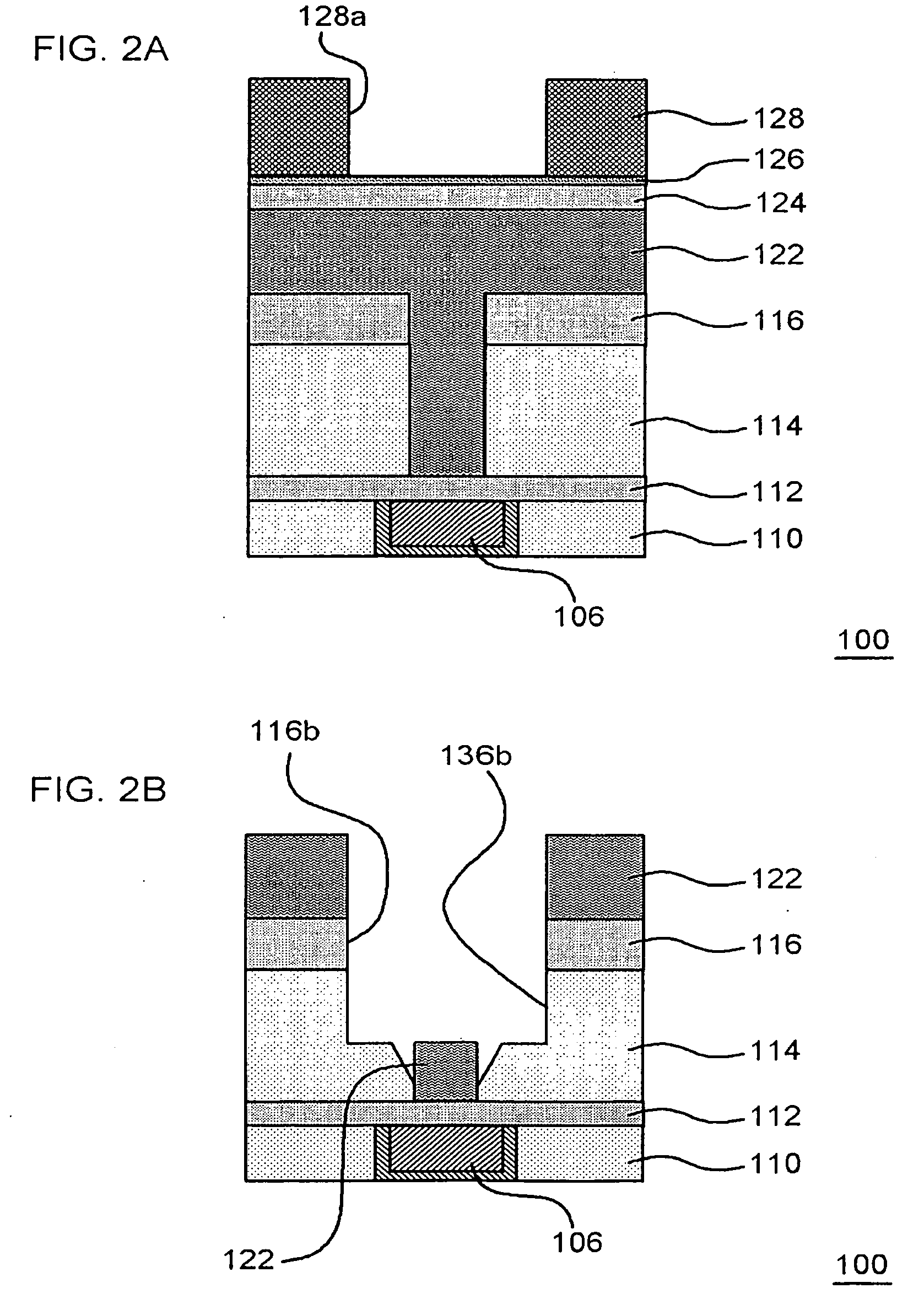
[0053]FIGS. 6A to 9 are cross-sectional views illustrating a procedure of manufacturing a semiconductor device according to the exemplary embodiment of the present invention. The exemplary embodiment of the present invention is different from the first exemplary embodiment of the present invention in the fact that a dual damascene trench is formed in a low dielectric constant layer by “trench first method”.

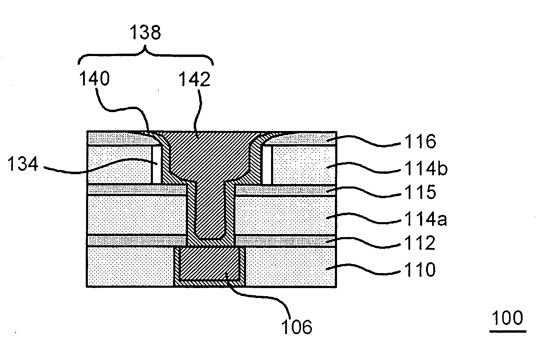
[0054]A semiconductor device 100 has a structure that an insulating interlayer 110 is formed on a substrate (not shown) which is a semiconductor substrate such as a silicon substrate, and a lower copper interconnect 106 is formed in the insulating interlayer 110. In such a semiconductor device 100, an etching stopper 112, a first low dielectric constant layer 114a, an etching stopper 115, a second low dielectric constant layer 114b, and a first protection insulating layer 116 are formed on the insulating interlayer 110 and the lower copper interconnect 106 in the described order.

[...


PUM


Abstract

A trench is formed by a process which removes a damage layer formed on a sidewall of a low dielectric constant layer, a process which forms a second protection insulating layer by a chemical vapor deposition (CVD) technique and forms a second concave portion by covering a sidewall of the low dielectric constant layer with the second protection insulating layer, and a process which shapes the second protection insulating layer by etch back so that a trench has a sidewall that the second protection insulating layer is selectively formed on a surface of the low dielectric constant layer.

Description

[0001]This application is based on Japanese patent application NO. 2008-278351, the content of which is incorporated hereinto by reference.BACKGROUND[0002]1. Technical Field[0003]The present invention relates to a semiconductor device and a method for manufacturing the same.[0004]2. Related Art[0005]Recently, a copper (Cu) interconnect having low resistance is usually being employed in an advanced semiconductor device pursuing down-scaling and high-speed operation. A copper interconnect is formed by a damascene process. In the damascene process, an interconnect is formed such that a concave portion is formed in an insulating interlayer, a barrier metal layer and a copper layer are formed in the concave portion to embed the concave portion, and portions of the copper layer and the barrier metal layer which are exposed outside the concave portion are removed by a chemical mechanical polishing (CMP) technique. A multi-layer interconnect structure is formed by repetitively performing th...

Claims


Application Information

Patent Timeline
IPC IPC(8): H01L23/52H01L21/467
CPCH01L21/02063H01L21/76804H01L21/76831H01L21/76814H01L21/76808
Inventor NISHIZAWA, ATSUSHI
Owner RENESAS ELECTRONICS CORP
Why Eureka
Try Eureka