Manufacturing method for raising new property of semiconductor element

A manufacturing method and semiconductor technology, applied in semiconductor/solid-state device manufacturing, semiconductor devices, electrical components, etc., can solve problems such as data disappearance

Inactive Publication Date: 2003-07-09
SK HYNIX INC
View PDF0 Cites 0 Cited by
  • Summary
  • Abstract
  • Description
  • Claims
  • Application Information

AI Technical Summary

Problems solved by technology

However, the initial charge amount stored in the capacitor may be consumed by leakage current generated in the

Method used


Image

  • Manufacturing method for raising new property of semiconductor element
  • Manufacturing method for raising new property of semiconductor element
  • Manufacturing method for raising new property of semiconductor element

Examples


Embodiment Construction

[0016] Hereinafter, preferred embodiments of the present invention will be described in detail with reference to the accompanying drawings.

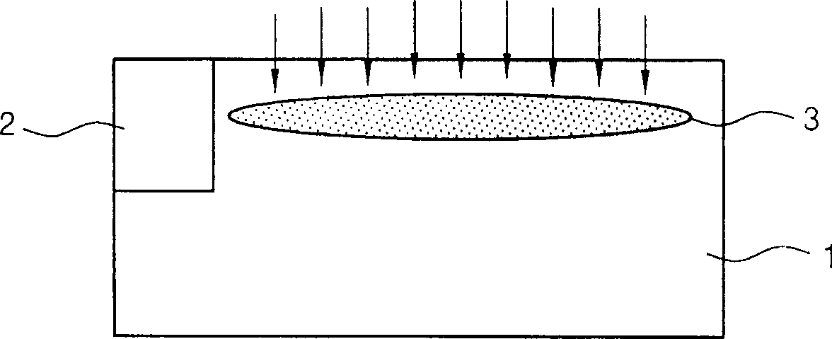
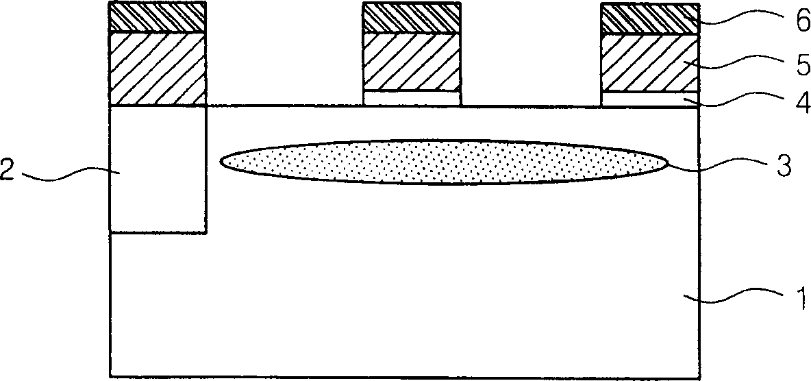
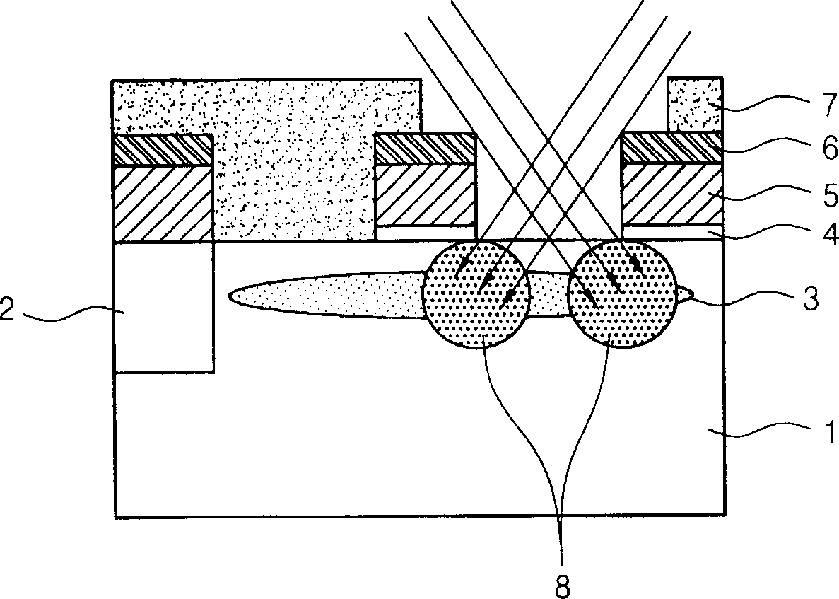
[0017] 1a to 1d are cross-sectional views for explaining the steps of the method of manufacturing a semiconductor element according to the embodiment of the present invention, and the description is as follows.

[0018] Referring to FIG. 1a, a trench-type element isolation film 2 defining its active region is formed on a semiconductor substrate 1 at an appropriate place by a known STI (Shallow Trench Isolation) process. Next, in order to adjust the threshold voltage (Vt) of the cell transistor, a predetermined impurity such as boron is ion-implanted into the active region of the semiconductor substrate 1 . At this time, the ion implantation for the adjustment of the threshold voltage is preferably performed within a range of 0 to 90% of the concentration of all dopants necessary for the adjustment of the threshold voltage. Symbol 3 in t...


PUM


Abstract

Disclosed is a method for fabricating a semiconductor device wherein boron-halo ion implantation is performed only to a bit-line contact part while masking a storage node contact part. The method comprises the steps of: performing a first ion implantation into the semiconductor substrate to control the threshold voltage Vt; forming a gate electrode on the semiconductor substrate in which the first ion implantation has been performed; performing a second ion implantation with a tilt of desired degree, using the gate electrode as a mask in order to control the threshold voltage; and performing a third ion implantation to form an LDD region in the substrate region at both sides of the gate electrode. In this method, the first ion implantation is performed at a range of below 90% of the whole doping concentration required to control the threshold voltage, and the second ion implantation is performed with a degree of below 30 DEG and in two directions or four directions vertical to the gate electrode.

Description

technical field [0001] The present invention relates to a method of manufacturing a semiconductor element, and more particularly to a method of manufacturing a semiconductor element capable of improving refresh characteristics due to reduced design standards. Background technique [0002] As is well known, a dynamic RAM (Dynamic Random Access Memory) element is a memory element in which stored data can be read when necessary, using metal-oxide-semiconductor transistors that act as switches and charges, i.e., capacitors that hold data A collection of dynamic RAM cells and the like are fabricated. [0003] In such a dynamic RAM element, the storage of data is equivalent to accumulating electric charge in a capacitor, and ideally, the electric charge accumulated in the capacitor is not consumed. However, the initial charge amount stored in the capacitor may be consumed by leakage current generated in the pn junction of the metal oxide semiconductor transistor, and as a result,...

Claims


Application Information

Patent Timeline
IPC IPC(8): H01L27/108H01L21/265H01L21/336H01L21/8234H01L21/8242
CPCH01L21/26586H01L29/66537H01L27/10873H01L21/823418H01L27/10855H01L21/823412H10B12/05H10B12/0335H10B12/00
Inventor 徐文植朴性桂
Owner SK HYNIX INC
Why Eureka
Try Eureka