Semiconductor device and method for manufacturing the same

a technology of semiconductors and semiconductors, applied in the direction of semiconductor devices, basic electric elements, electrical equipment, etc., can solve the problems of gate induced drain leakage (gidl), short channel effect, information stored in the dram is lost, etc., to reduce gidl, improve refresh characteristics, and suppress the effect of gate induced drain leakag

Active Publication Date: 2012-03-15
SK HYNIX INC
View PDF7 Cites 3 Cited by
  • Summary
  • Abstract
  • Description
  • Claims
  • Application Information

AI Technical Summary

Benefits of technology

[0007]An embodiment of the present invention relates to a semiconductor device and a method for manufacturing the same, in which a recess gate structure is formed in a region where a gate and a source / drain overlap so as to suppress an increase in gate induced drain leakage (GIDL), and a gate insulation film is more thickly deposited in a region having weak GIDL, resulting in reduction of GIDL, thus improving refresh characteristics due to leakage current.

Problems solved by technology

The DRAM allows information to be read therefrom and written thereon, but information stored in the DRAM is lost unless the information is periodically rewritten within a designated period while power is supplied.
When the channel length of the device is shortened, a short channel effect and gate induced drain leakage (GIDL) can occur.
However, increasing gate channel length causes problems, such as increasing gate resistance and deterioration of GIDL at a region where a gate and a source / drain region overlap with each other.

Method used


Image

  • Semiconductor device and method for manufacturing the same
  • Semiconductor device and method for manufacturing the same
  • Semiconductor device and method for manufacturing the same

Examples


Embodiment Construction

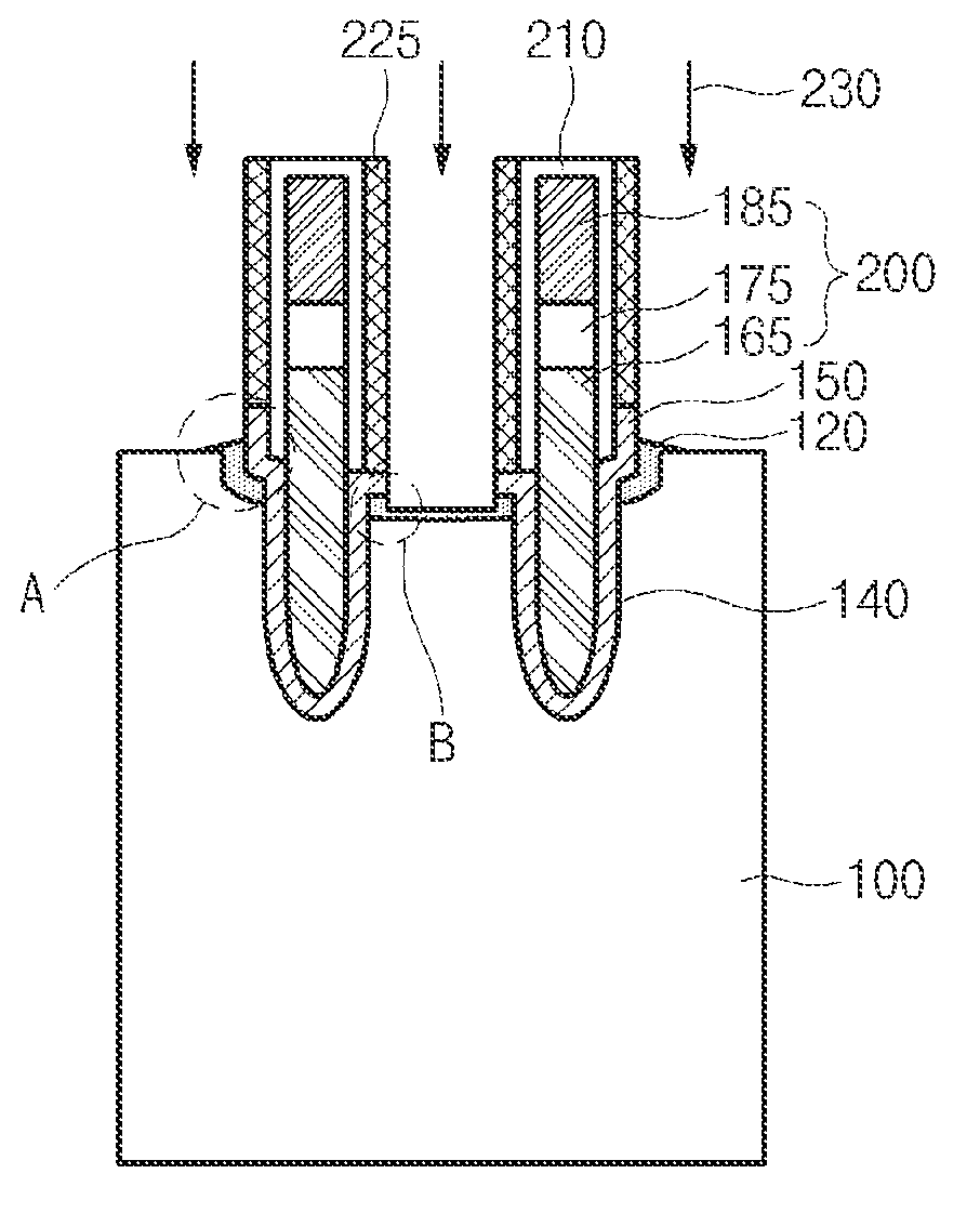
[0023]Reference will now be made in detail to embodiments of the present invention, examples of which are illustrated in the accompanying drawings. Wherever possible, the same reference numbers will be used throughout the drawings to refer to the same or like parts. A semiconductor device and a method for manufacturing the same according to embodiments of the present invention will hereinafter be described with reference to the appended drawings.

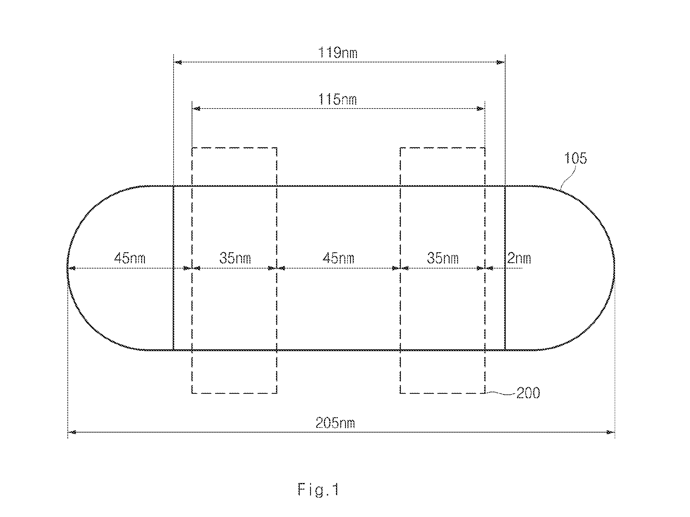
[0024]FIG. 1 is a plan view illustrating a semiconductor device and a method for manufacturing the same according to an embodiment of present invention.

[0025]Referring to FIG. 1, an active region 105 and recess gate patterns 200 are formed over a semiconductor substrate.

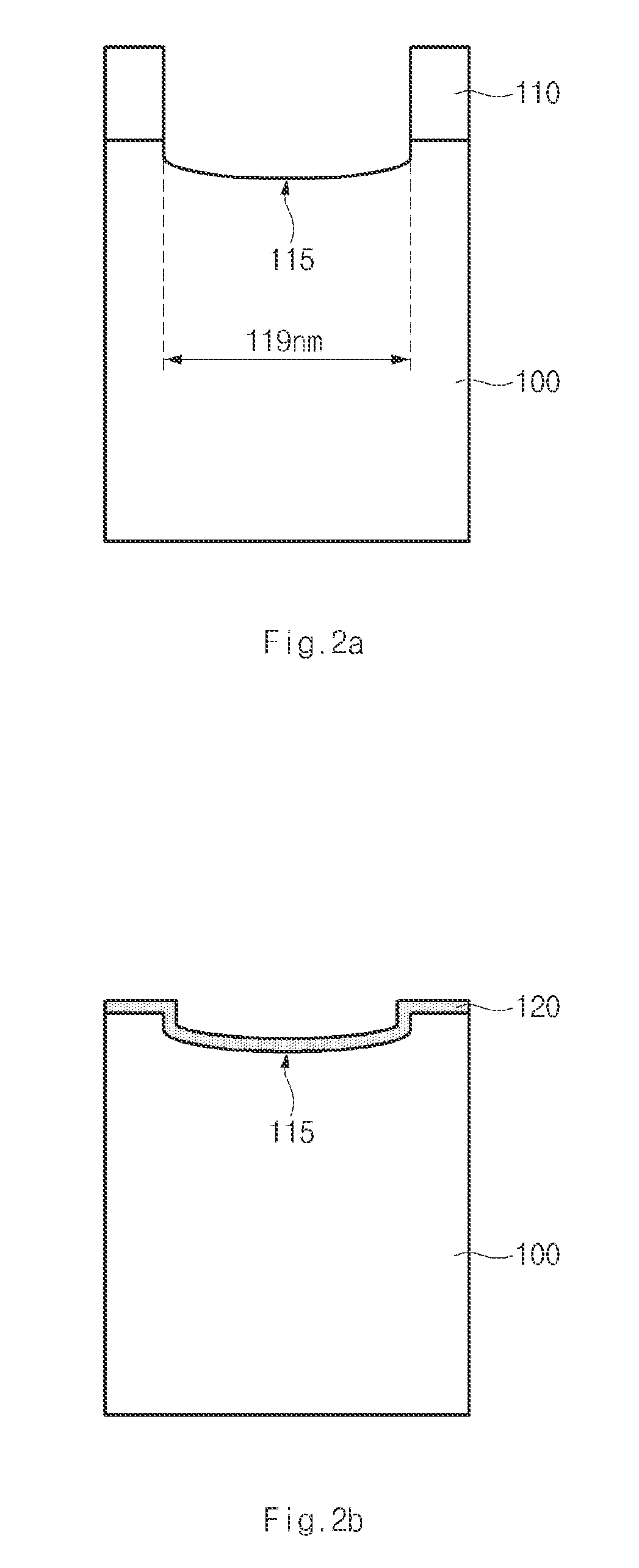
[0026]In accordance with one embodiment, as shown in FIG. 1, the active region 105 is formed to have a width of 205 nm in the horizontal direction and the recess gate patterns 200 are formed to have a width of 35 nm in the horizontal direction. Here, first recesses are formed...


PUM


Abstract

A semiconductor device and a method for manufacturing the same are disclosed. A recess gate structure is formed between an overlapping region between a gate and a source/drain so as to suppress increase in gate induced drain leakage (GIDL), and a gate insulation film is more thickly deposited in a region having weak GIDL, thereby reducing GIDL and thus improving refresh characteristics due to leakage current.

Description

CROSS-REFERENCE TO RELATED APPLICATION[0001]The priority of Korean patent application No. 10-2010-0089441 filed on Sep. 13, 2010, the disclosure of which is hereby incorporated in its entirety by reference, is claimed.BACKGROUND OF THE INVENTION[0002]Embodiments of the present invention relate to a semiconductor device and a method for manufacturing the same.[0003]In general, semiconductor memories, which store information such as data or commands of programs, include a DRAM and a SRAM. A DRAM is a memory in which stored data may be read and other information may be stored. The DRAM allows information to be read therefrom and written thereon, but information stored in the DRAM is lost unless the information is periodically rewritten within a designated period while power is supplied. Although a DRAM needs to be refreshed in this way, it has a low price per memory cell and a high integration density, and is thus widely used as a high capacity memory.[0004]A metal-oxide semiconductor ...

Claims


Application Information

Patent Timeline
Patent Type & Authority Applications(United States)
IPC IPC(8): H01L29/78H01L21/28
CPCH01L27/10876H01L29/66659H01L29/66621H01L29/4236H10B12/053H01L29/7835
Inventor CHUNG, WOO YOUNG
Owner SK HYNIX INC
Why Eureka
Try Eureka