Semiconductor memory device

a memory device and semiconductor technology, applied in the field of semiconductor memory devices, can solve the problems of increasing the voltage output of the ref-cell cell/sub>ref /sub>, the voltage output of the ref-cell cell/sub>is not enough for the sense amplifier to operate with high stability, and the difficulty of amplifying the difference of potential between bit lines potential with high accuracy, etc., to achieve the effect of suppressing the increase of current consumption and high stability

Active Publication Date: 2008-09-11
RENESAS ELECTRONICS CORP
View PDF3 Cites 0 Cited by
  • Summary
  • Abstract
  • Description
  • Claims
  • Application Information

AI Technical Summary

Benefits of technology

[0015]As a result of decreasing a number of transistors for inputting a boosted voltage to a gate, it is possible to suppress an increase of current consumption in a voltage-boosting circuit and make a sense amplifier operable with high stability.

Problems solved by technology

Therefore, in the above-mentioned half VDD precharge method, it is difficult for a sense amplifier to amplify a difference of potential between bit lines potential with high accuracy, because the precharged level is close to a threshold level of the sense amplifier.
Therefore, it is needed to activate a voltage-boosting circuit for raising the potential level of the three word lines, thereby increasing an amount of current consumption.
But, there are cases where a voltage output from the ref-cell CELLRef is not enough for the sense amplifier to operate with high stability because of an tolerance of the capacitance of the main cell CELLT and the ref-cell CELLRef.
In case of using the GND precharge method, an amount of current consumption is increased, and it is difficult to make the sense amplifier operable with high stability because of the tolerance between circuit elements.

Method used


Image

  • Semiconductor memory device
  • Semiconductor memory device
  • Semiconductor memory device

Examples


first embodiment

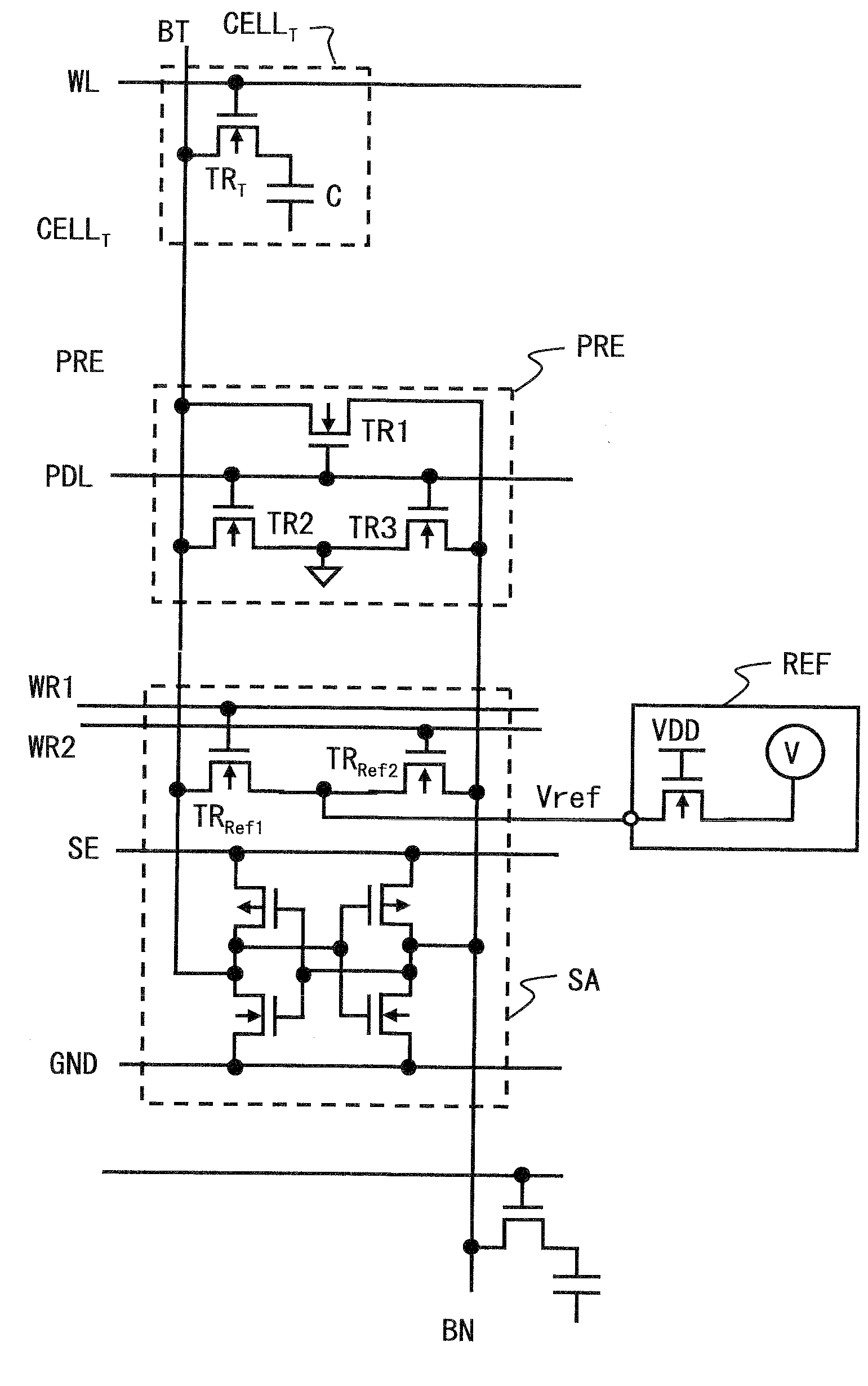
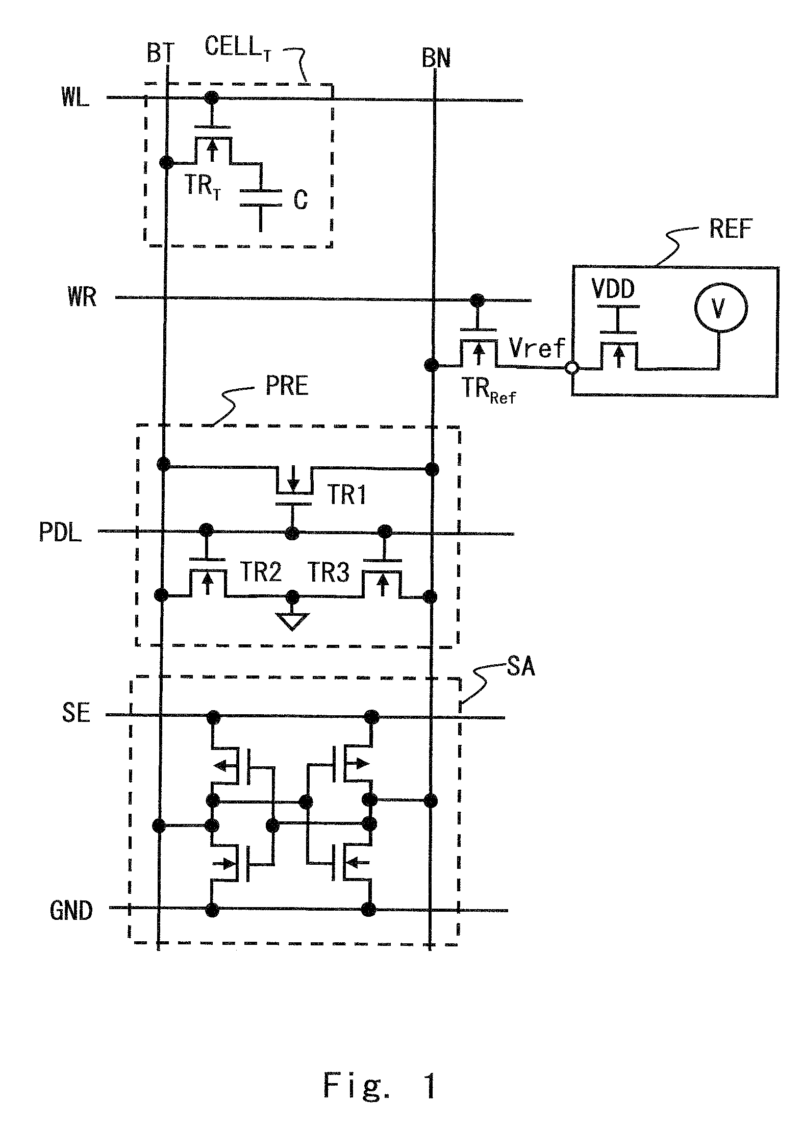
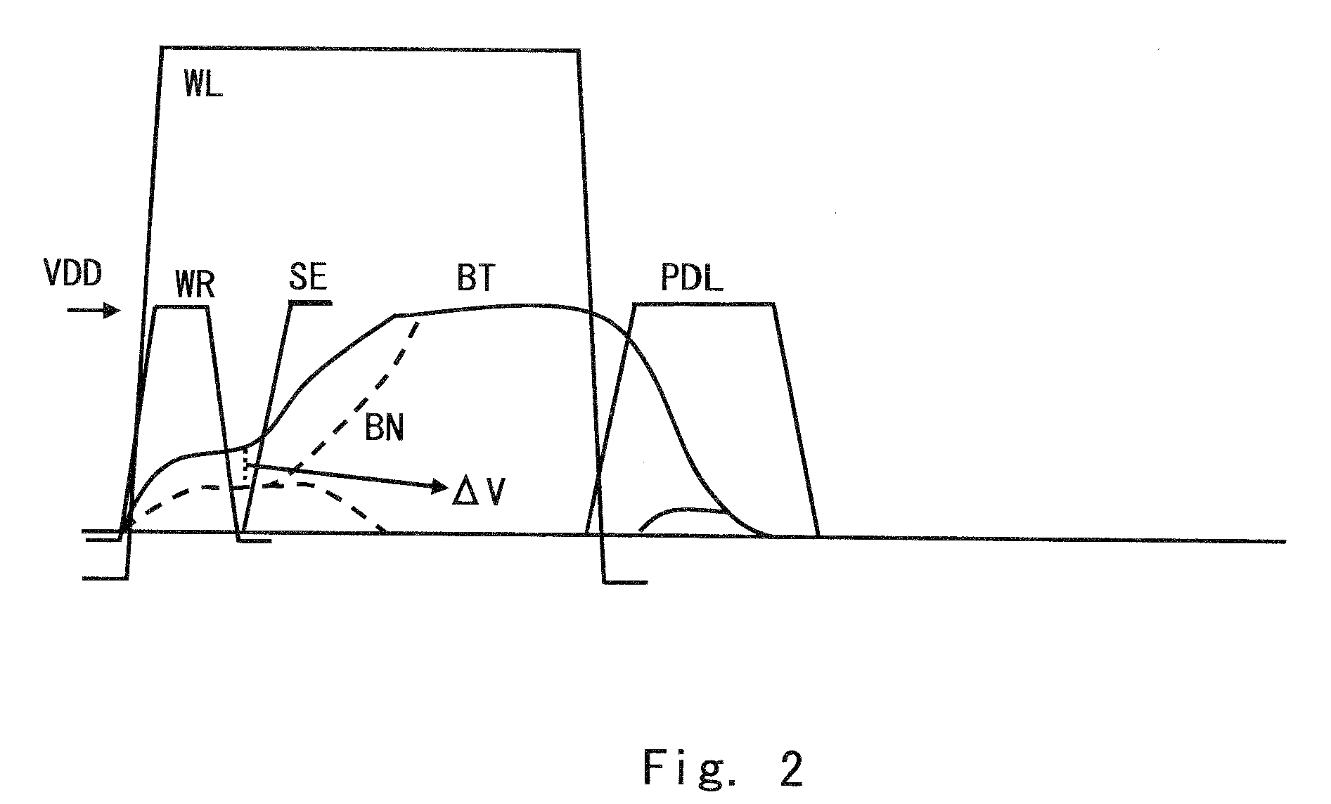
[0027]A first embodiment of this invention is explained below with references to drawings. FIG. 1 is a view showing a circuit of one of a bit line pair of a DRAM of this embodiment. As shown in FIG. 1, the DRAM of this embodiment includes bit lines BT, BN, a memory cell CELLT, a transistor for supplying a reference voltage (a reference voltage supply switch) TRRef, a precharge circuit PRE, a sense amplifier SA, and a reference voltage generation circuit REF. Note that the memory cell CELLT memorizes data and hereinafter referred to as a main cell.

[0028]The main cell CELLT is comprised of an n-mos (n-type Metal Oxide Semiconductor) transistor TRT and a capacitor C. A gate of the transistor TRT of the main cell CELLT is connected to a word line WL. One of a source or drain of the main cell CELLT is connected to a bit line BT and the other is connected to the capacitor C. The main cell CELLT memorizes a logical value of H or L by storing charge in the capacitor C. When the charges stor...

second embodiment

[0051]A second embodiment of this invention is explained below with references to drawings. A plurality of memory cells are connected to one sense amplifier in an actual DRAM. FIGS. 4A and 4B each shows an exemplary layout of connecting the plurality of memory cells to one sense amplifier. Note that the precharge circuit and other elements are omitted in FIGS. 4A and 4B, because FIGS. 4A and 4B are views for explaining exemplary layouts.

[0052]FIG. 4A shows a layout of a folded bit arrangement where a bit line pair is arranged at one side of the sense amplifier. As shown in FIG. 4A, the sense amplifier SA is shared among the bit line pair BT1 and BN1 at the right side and the bit line pair BT2 and BN2 at the left side. Note that, the words indicating the directions are used on the assumption that the drawings are seen in front.

[0053]FIG. 4B shows a layout of an open bit arrangement where a bit line pair is formed by arranging a bit line BT at the left side of the sense amplifier and ...

third embodiment

[0069]FIG. 7 is a circuit diagram showing a bit line pair of a memory cell of the third embodiment of this invention. The same components as those of FIGS. 1 and 5 are denoted by identical reference numerals and undue explanation is omitted. The memory of this embodiment adopts the folded bit arrangement as shown in FIG. 4A.

[0070]The difference between the circuit of FIG. 5 and the circuit of FIG. 7 is that it is possible to input signals to each of the bit line pair selection transistors TR4 to TR7 for independently controlling the conductive states of each transistors TR4 to TR7.

[0071]As a result of adopting this configuration, only the TG1 is set to H level and only the transistor TR4 is set to be conductive in accessing the main cell CELLT that is connected to the bit line BT as shown in FIG. 7 for example. Other control signals TG2 to TG4 are set to L level and non-conductive states are sustained.

[0072]In the condition explained above, not all the bit line pairs BN1 are set to ...


PUM


Abstract

In one embodiment, a semiconductor memory device includes a plurality of pairs of bit lines, each of the pairs including a first bit line, a second bit line, a memory cell coupled to the first bit line, a sense amplifier determining the logical value stored in the memory cell according to a potential difference between the first and the second bit line, a reference voltage generation circuit, and a reference voltage supply switch coupling an output of the reference voltage generation circuit to the second bit line.

Description

BACKGROUND OF THE INVENTION[0001]1. Field of the Invention[0002]The present invention relates to a semiconductor memory device and in particular to a Dynamic Random Access Memory (hereinafter referred to as a DRAM).[0003]2. Description of Related Art[0004]A DRAM cell that stores data using a capacitor has been widely known as a semiconductor memory device. In the DRAM, a precharge operation is carried out to set a potential level of each bit lines to a predetermined level before reading or writing data.[0005]A half VDD precharge method is generally used as the precharge method. A potential level of each bit lines is set to about a half potential of a power supply potential VDD in the half VDD precharge method. As the power supply voltage VDD becomes lower, the level set by the precharge method also becomes lower in these days. Therefore, in the above-mentioned half VDD precharge method, it is difficult for a sense amplifier to amplify a difference of potential between bit lines pote...

Claims


Application Information

Patent Timeline
Patent Type & Authority Applications(United States)
IPC IPC(8): G11C7/00
CPCG11C7/065G11C7/12G11C11/4099G11C11/4091G11C11/4094G11C7/14
Inventor TAKAHASHI, HIROYUKINAKAGAWA, ATSUSHI
Owner RENESAS ELECTRONICS CORP
Why Eureka
Try Eureka