Semiconductor device and method for manufacturing the same

a semiconductor memory device and semiconductor technology, applied in the field of semiconductor memory devices, can solve the problems of reducing the refresh characteristics of the semiconductor memory device, affecting the operation deteriorating the gidl so as to improve the refresh characteristics of the semiconductor device and reduce the work function.

Active Publication Date: 2014-11-04
SK HYNIX INC
View PDF6 Cites 1 Cited by
  • Summary
  • Abstract
  • Description
  • Claims
  • Application Information

AI Technical Summary

Benefits of technology

[0009]An embodiment of the present invention relates to a semiconductor device and a method for manufacturing the same in which a line-type buried gate is formed by burying a non-operating gate (isolation gate) with a polysilicon material to reduce a work function and a Gate Induced Drain Leakage (GIDL) caused by the non-operating gate, resulting in improvement of refresh characteristics of the semiconductor device.

Problems solved by technology

However, if the concentration of the impurities doped into the channel region is increased while the design rule is reduced to 100 nm or less, the electric field of a Storage Node (SN) junction is increased, thereby lowering the refresh characteristics of a semiconductor memory device.
As a result, there may arise shortcomings in which parasitic capacitance is increased such that an operating margin of a sense amplifier (sense-amp) that amplifies data transmitted via the bit line is deteriorated, resulting in a negative influence upon operation of the semiconductor device.
First, GIDL characteristics of a semiconductor device are deteriorated between a conductive material (gate electrode) and an N-type junction of an active region.
Second, refresh characteristics of the whole semiconductor device are deteriorated due to the deteriorated GIDL characteristics.

Method used


Image

  • Semiconductor device and method for manufacturing the same
  • Semiconductor device and method for manufacturing the same
  • Semiconductor device and method for manufacturing the same

Examples


Embodiment Construction

[0032]Reference will now be made in detail to embodiments of the present invention, examples of which are illustrated in the accompanying drawings. Wherever possible, the same reference numbers will be used throughout the drawings to refer to the same or like parts.

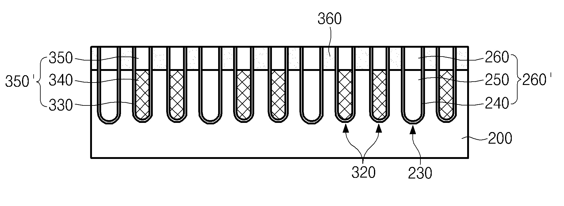
[0033]FIG. 1 is a plan view illustrating a semiconductor device and a method for manufacturing the same according to an embodiment of the present invention.

[0034]Referring to FIG. 1, a device isolation region 225 defining an active region 215, and buried gates 260′ and 350′ crossing the active region 215 are formed over a semiconductor substrate 200. In an embodiment, the active region 215 is formed as an island type, and each buried gate 260′ or 350′ includes an operating gate 350′ and a non-operating gate 260′ and is formed as a line type.

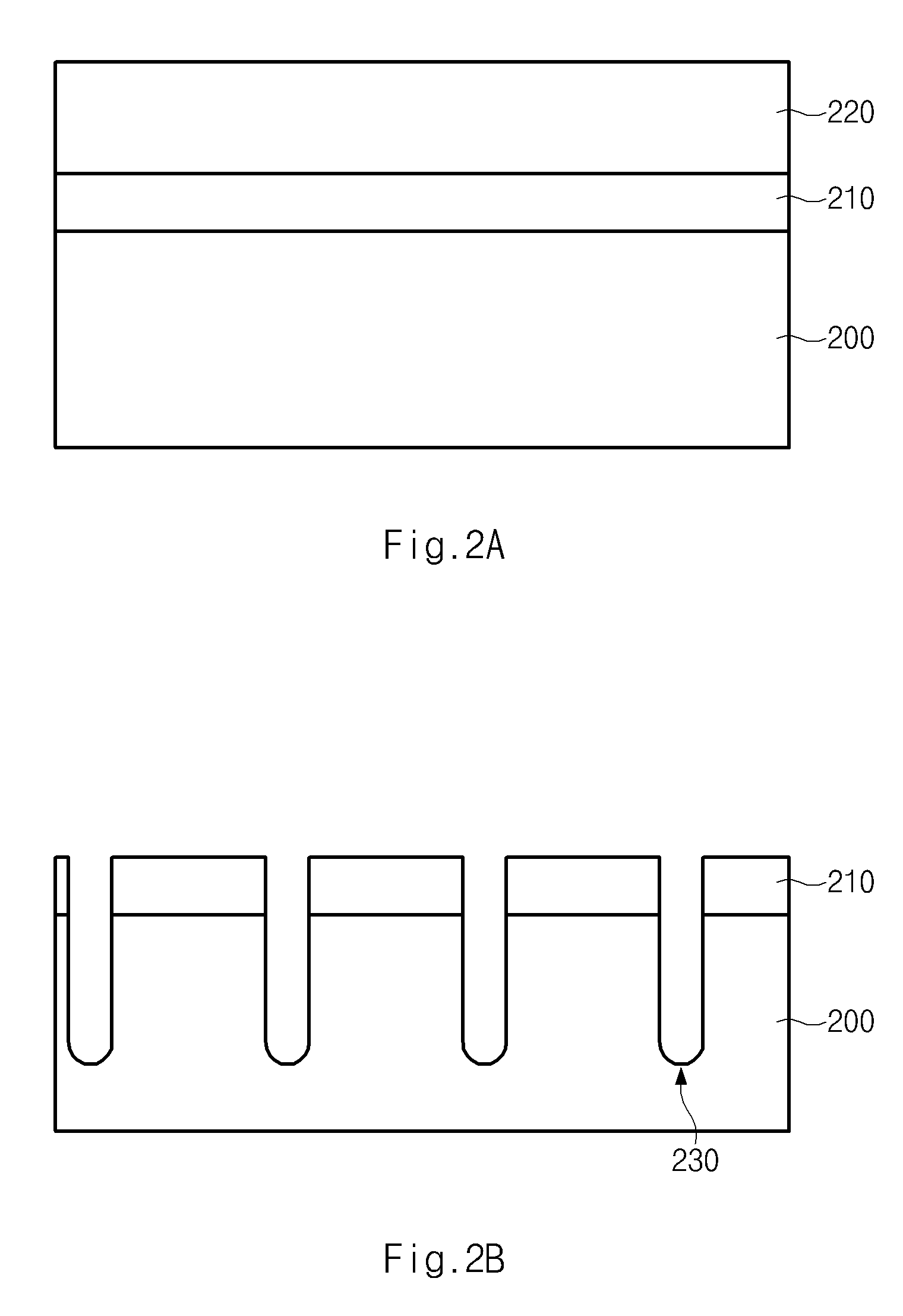
[0035]The device isolation region 225 for defining an active region 215 is formed as described below.

[0036]A pad insulation film (not shown) comprising a pad oxide film and a pad nitri...


PUM


Abstract

In the semiconductor device, a line-type buried gate is formed by burying a non-operating gate (isolation gate) with a polysilicon material to reduce a work function and a Gate Induced Drain Leakage (GIDL) caused by the non-operating gate, resulting in improvement of refresh characteristics of the semiconductor device. Operating gates including a metal conductive material may be formed in a separate step.

Description

CROSS-REFERENCE TO RELATED APPLICATION[0001]The priority of Korean patent application No. 10-2011-0130830 filed on 8 Dec. 2011, the disclosure of which is hereby incorporated in its entirety by reference, is claimed.BACKGROUND OF THE INVENTION[0002]Embodiments of the present invention relate to a semiconductor device and a method for manufacturing the same in which a line-type buried gate is formed by burying a non-operating gate (isolation gate) with a polysilicon material.[0003]A semiconductor memory device includes a plurality of unit cells each having a capacitor and a transistor. The capacitor is used to temporarily store data, and the transistor is used to transfer data between a bit line and the capacitor in response to a control signal (word line). The data transfer occurs using a semiconductor property wherein an electrical conductivity changes depending on conditions. The transistor has three regions: a gate, a source, and a drain. Electric charges are moved between the so...

Claims


Application Information

Patent Timeline
Patent Type & Authority Patents(United States)
IPC IPC(8): H01L29/78H01L21/762H01L29/66H01L27/108
CPCH01L21/762H01L27/10876H01L27/10823H01L29/66666H01L27/10891H01L29/7827H01L21/76H01L21/28123H01L29/7813H10B12/34H10B12/053H10B12/488H10B99/00
Inventor KIM, KYUNG, DO
Owner SK HYNIX INC
Why Eureka
Try Eureka