Method and system for spectral stitching of tunable semiconductor sources

a technology of semiconductor sources and spectroscopy, applied in the field of tunable source spectroscopy systems, can solve the problems of reducing or degrading power of tunable signals, and achieve the effect of widening the scan band

Active Publication Date: 2008-01-29
EXCELITAS TECH
View PDF11 Cites 25 Cited by
  • Summary
  • Abstract
  • Description
  • Claims
  • Application Information

AI Technical Summary

Benefits of technology

[0010]A control system compensates for the spectral roll-off of the at least two semiconductor sources over the combined scan band. In this way, the system can produce an effectively wider scan band by combining the output from two semiconductor sources, without incurring penalities associated with available power in the tunable optical signals near the limits of the spectral bands of the separate semiconductor sources.

Problems solved by technology

Specifically, near the limits of the semiconductor sources' spectral bands, the power in the tunable signal tends to degrade or decrease.

Method used


Image

  • Method and system for spectral stitching of tunable semiconductor sources
  • Method and system for spectral stitching of tunable semiconductor sources
  • Method and system for spectral stitching of tunable semiconductor sources

Examples


second embodiment

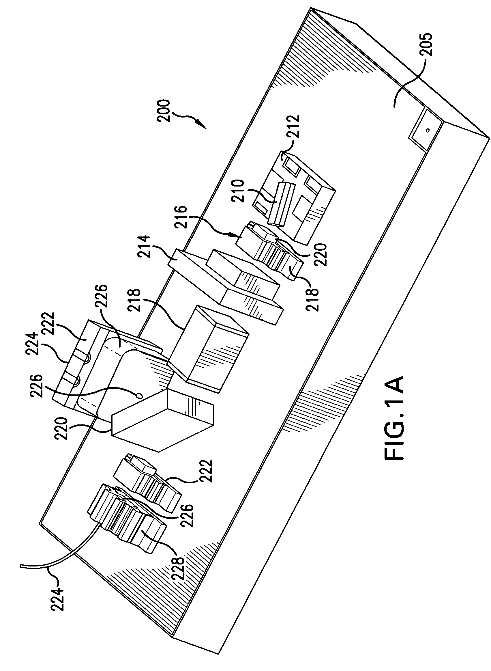
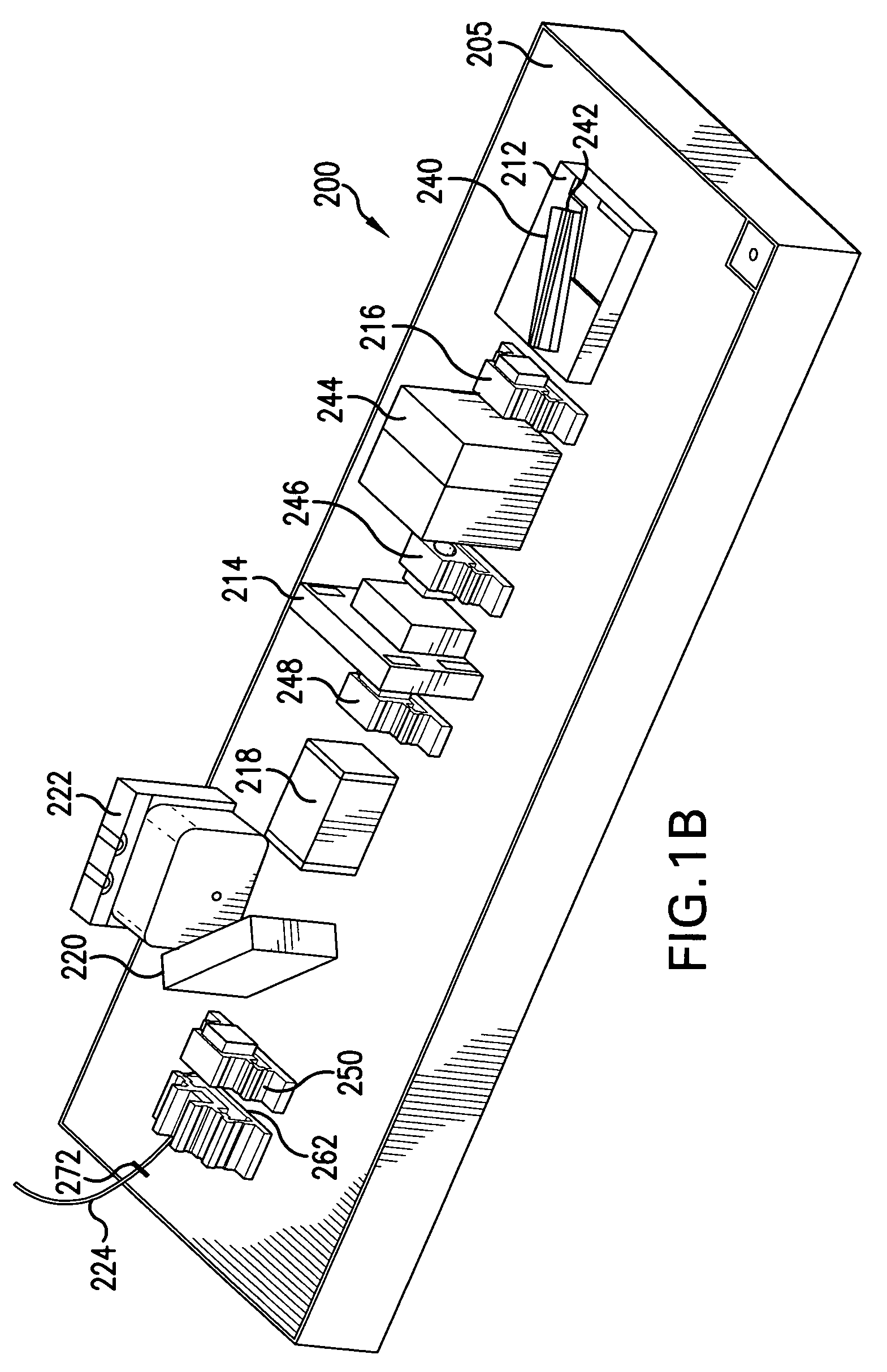
[0037]FIG. 1B illustrates the tunable semiconductor source 200. In this embodiment, the tunable semiconductor source 200 again comprises an optical bench 205.

[0038]Instead of the SLED chip, however, a semiconductor optical amplifier (SOA) chip 240 is used as the semiconductor gain medium. This chip is also secured to the bench 205 via a submount 212.

[0039]In the illustrated embodiment, the SOA chip 240 is a reflective SOA. Specifically, the SOA chip's back facet 242 has a reflective coating in order to function as a back reflector of the laser cavity of the semiconductor source 200.

[0040]Light exiting from the SOA chip 240 is columnated by a first lens component 216. It passes through an isolator at 244 to a second lens component 246 and then to a tunable filter 214.

[0041]The filter 214 functions to control which of the longitudinal optical nodes have a net gain in the laser cavity of the laser tunable semiconductor tunable source 200.

[0042]Light exiting from the filter 214 is colli...

first embodiment

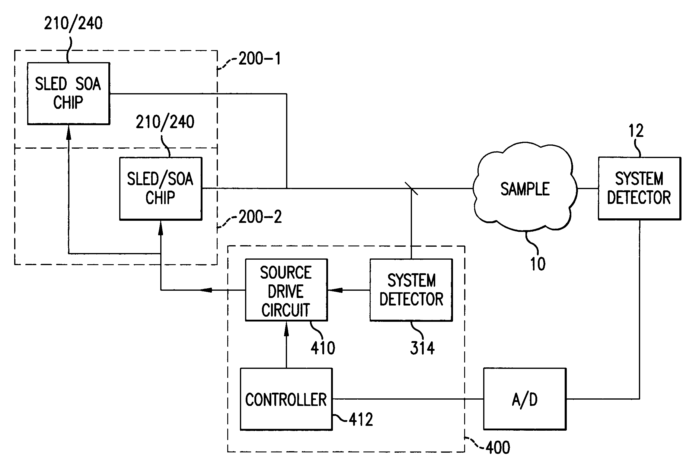
[0058]FIG. 4 illustrates a first embodiment control system for compensating for the spectral roll-off of the at least two semiconductor sources, e.g., SLED sources 210 or SOA sources 240, over the combined scan band provided by the combination of the tunable signals from the two semiconductor sources 200-1, 200-1.

[0059]Specifically, source one 200-1 is driven by a source drive circuit of a control system 400 including a system detector 314 and a controller 412. In other embodiments, instead of using the system detector 314, the source detectors 224 are used to sample the magnitude of the signals produced by the sources 200-1, 200-2.

[0060]The source drive circuit 410 controls the current to the diode chips, e.g., SLED chips 210 of the tunable SLED of FIG. 1A, or SOA chips 240 of the tunable lasers of FIG. 1B, 1C. The modulation of the drive current maintains the levels of the respective tunable signals at a fixed level such as level 450 of FIG. 3. Specifically, near the limits of the...


PUM


Abstract

A multi semiconductor source tunable spectroscopy system has two or more semiconductor sources for generating tunable optical signals that are tunable over different spectral bands. The system enables the combination of these tunable signals to form an output signal that is tunable over a combined band including these individual spectral bands of the separate semiconductor sources. The system further compensates for spectral roll-off associated with the semiconductor sources. Specifically, near the limits of the semiconductor sources' spectral bands, the power in the tunable signal tends to degrade or decrease. The system compensates for this roll-off using drive current control, attenuators, or electronic compensation.

Description

RELATED APPLICATIONS[0001]This application is a continuation in part of to application Ser. No. 10 / 953,046, filed on Sep. 29, 2004, by Flanders, et al., now U.S. Pat. No. 7,157,712 which application is incorporated herein by this reference in its entirety.BACKGROUND OF THE INVENTION[0002]A number of general configurations are used for tunable source spectroscopy systems. The lasers have advantages in that very intense tunable optical signals can be generated. A different configuration uses the combination of a broadband source and a tunable passband filter, which generates the narrowband signal that illuminates the sample.[0003]Historically, most tunable lasers were based on solid state gain media. While often powerful, these systems typically have high power consumptions. In contrast, tunable semiconductor laser systems have the advantage of relying on small, efficient, and robust semiconductor sources. One configuration uses semiconductor optical amplifiers (SOAs) and microelectro...

Claims


Application Information

Patent Timeline
Patent Type & Authority Patents(United States)
IPC IPC(8): H01S3/10
CPCG01J3/10
Inventor FLANDERS, DALE C.ATIA, WALID A.KUZNETSOV, MARK E.
Owner EXCELITAS TECH
Why Eureka
Try Eureka