Method and apparatus for determining probing locations for a printed circuit board

a printed circuit board and probing location technology, applied in the direction of printed circuit testing, instruments, computing, etc., can solve the problem that the maximum board flex may still exceed the safe limits, and achieve the effect of reducing the calculation time and minimizing the board flex

Inactive Publication Date: 2008-01-29
AGILENT TECH INC
View PDF5 Cites 5 Cited by
  • Summary
  • Abstract
  • Description
  • Claims
  • Application Information

AI Technical Summary

Benefits of technology

[0013]The present invention is a technique for optimizing the layout of probing locations for a PCB with a view to minimizing board flex when mounted in a tester fixture customized to test the PCB. The invention applies plate problem principles used in techniques previously reserved for post-probing-location selection tasks such as determination of board pusher and board retainer locations for minimizing board flex, and applies the principles during the probing location selection phase. The final probe layout of the fixture is therefore “pre-optimized” in terms of minimizing board flex by the locations of the probes themselves, thereby reducing the calculation time for determining, and corresponding number of, board pusher and retainer locations after the probing location selection is completed.
[0015]The probing location selection algorithm may be used to select probing locations for PCBs to be mounted in tester fixtures that allow either single-side probing only or dual-side probing. If the tester and fixture accommodates probing on both the bottom side and the top side of the PCB, the probing location selection algorithm will preferably attempt to balance the distribution of probing locations to both sides of the PCB so that the forces applied by probes on both sides of the PCB preferably cancel each other out or result in minimum board flex. Dual-side probing affords the additional advantage that the probes themselves can be used to counteract forces from opposite side probes, thereby reducing the need for and number of board pushers.

Problems solved by technology

Once the probing location selection algorithm has determined the optimal probe layout, the maximum board flex may still exceed safe limits.

Method used


Image

  • Method and apparatus for determining probing locations for a printed circuit board
  • Method and apparatus for determining probing locations for a printed circuit board
  • Method and apparatus for determining probing locations for a printed circuit board

Examples


Embodiment Construction

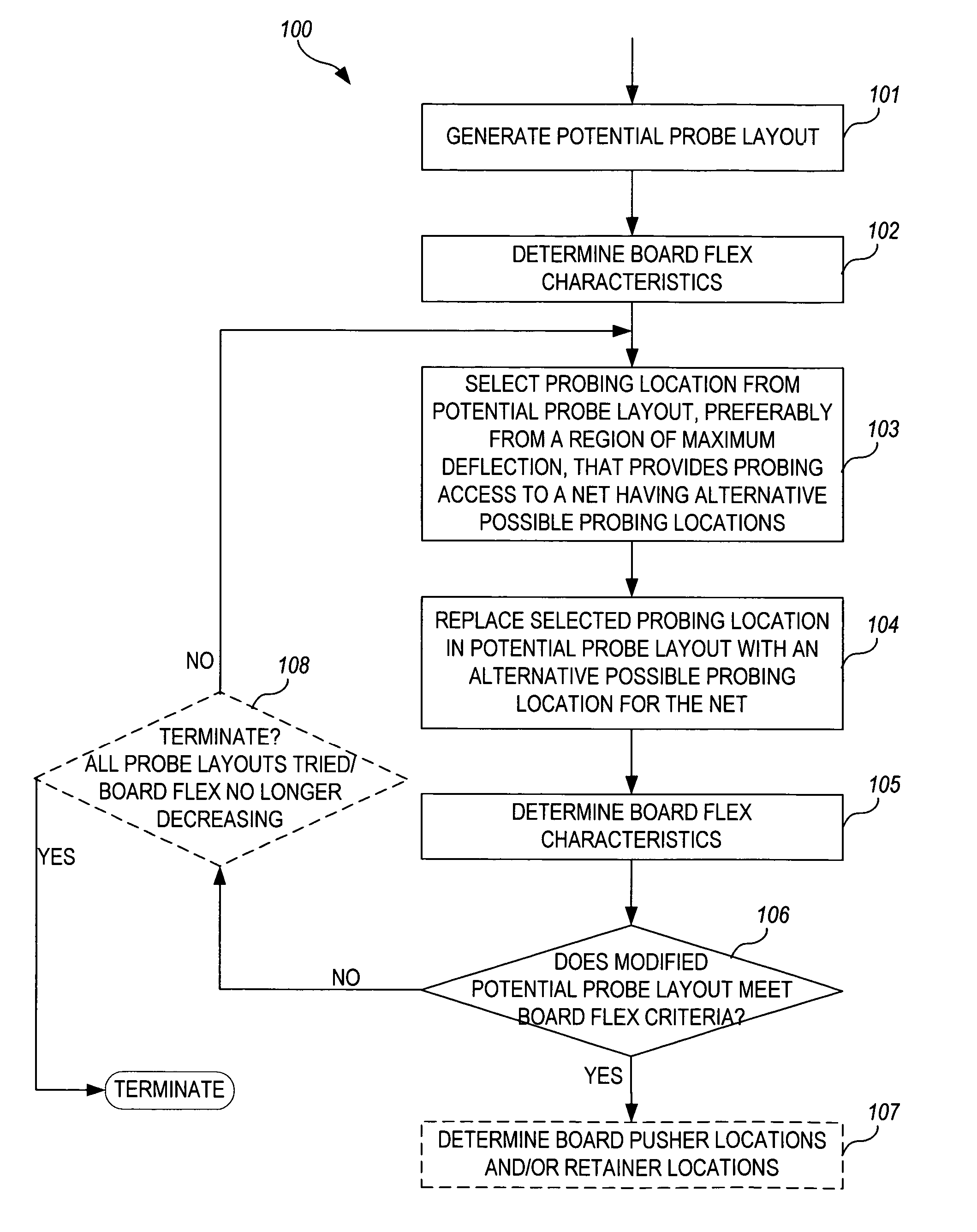
[0026]For purposes of clarity, the following terms are defined:

[0027]“net”—a signal transmission line which passes signals between two or more endpoints over an electrically conductive path; may be implemented as one or more of any of, including combinations of, the following: a trace, a via, a wire, a component lead, a solder ball, a wire bond, or any other electrically conductive element electrically connected between the two or more endpoints and through which the signal passes;

[0028]“test pad”—a point on a net accessible for probing, typically characterized by a surface area large enough to accommodate a probe head;

[0029]“probing location”—a test pad that is or is selected to be probed;

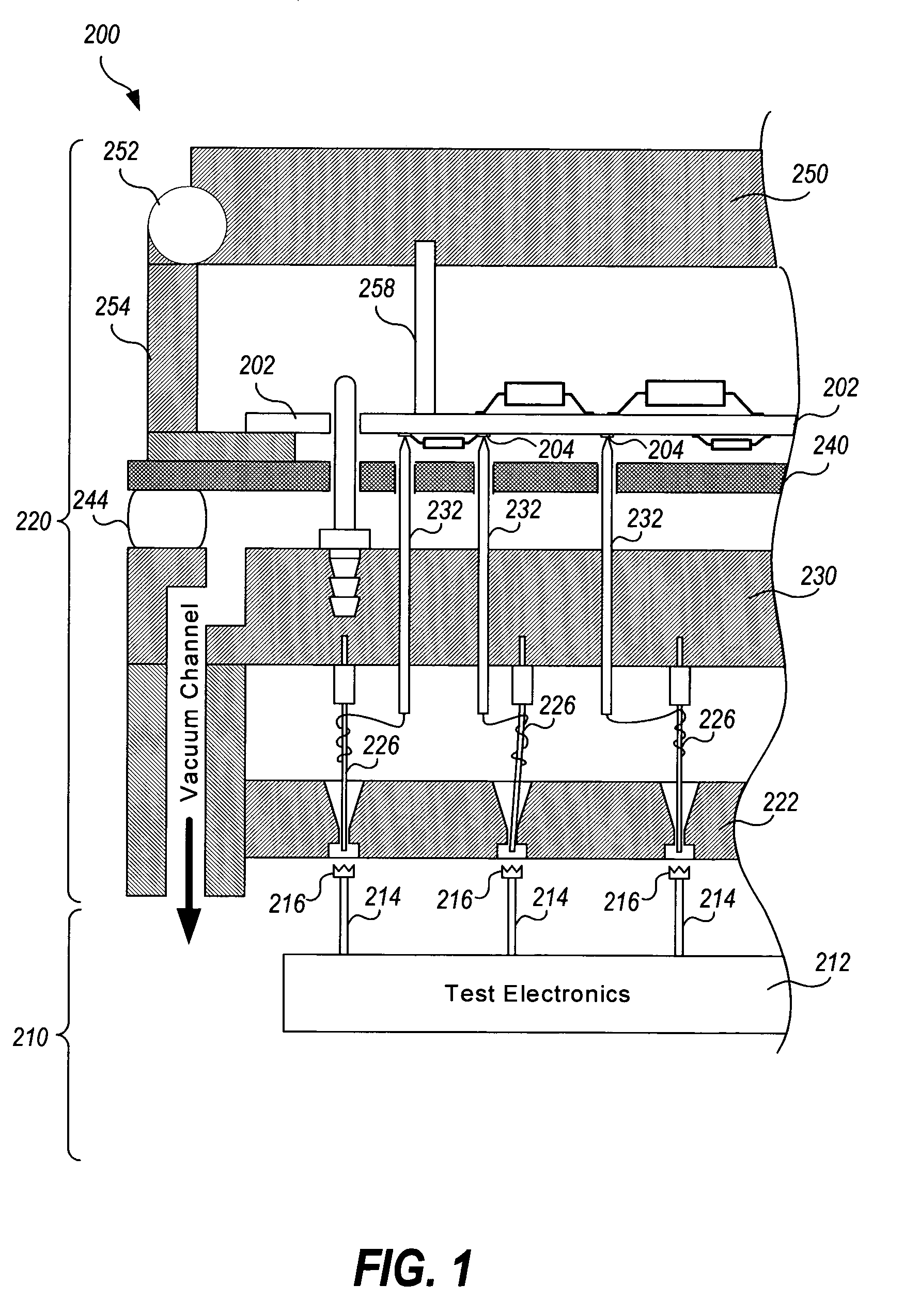
[0030]“fixture probe”—an electrically conductive element of a tester fixture which operates as a passive transmission line at least between a first end and a second end of the electrically conductive element, the first end configured to electrically contact a test pad of a circuit and the second e...


PUM


Abstract

Techniques for automating probing location selection during printed circuit board (PCB) and corresponding PCB tester fixture design are presented. The invention includes a system and algorithm for selecting a probe layout comprising a set of probing locations for a printed circuit board design having a plurality of nets, at least some of which have a number of alternative possible probing locations. The system and algorithm iteratively generates a potential probe layout comprising one or more probing locations per net, and based on the potential probe layout, determines one or more regions of maximum deflection. A probing location from the potential probe layout that is located in a region of maximum deflection and is associated with a net having one or more alternative probing locations is removed from the potential probe layout and replaced in the with one of the one or more alternate probing locations associated with the net. Regions of maximum deflection are recalculated based on the modified potential probe layout, and the replacement process is repeated until respective magnitudes of the respective areas of maximum deflection are below a threshold value.

Description

BACKGROUND OF THE INVENTION[0001]The present invention relates generally to printed circuit board design and testing, and more particularly to techniques for determining probing locations on a printed circuit board for tester access.[0002]Electronic products typically contain at least one printed circuit board (PCB). A PCB generally includes a number of electronic components that are electrically connected together by electrical paths called “nets” that are formed of various combinations of conductive traces, vias, wires, and solder, to form an operational circuit that performs a given function. A conventional PCB development cycle includes PCB design, test development, and tester fixture development.[0003]Where possible, given the state of the art of available development tools in the market, many steps involved in PCB design, test development and fixture development are automated, either fully or at least partially. For example, large automated industrial CAD development systems h...

Claims


Application Information

Patent Timeline
Patent Type & Authority Patents(United States)
IPC IPC(8): G06F17/50
CPCG01R31/2801
Inventor JACOBSEN, CHRIS R.PARKER, KENNETH P.
Owner AGILENT TECH INC
Why Eureka
Try Eureka