

Semiconductor package
a technology of semiconductors and packages, applied in semiconductor devices, semiconductor/solid-state device details, electrical apparatus, etc., can solve the problems of limiting the minimum size of dies and the manufacturing process can be more complex than mcms, and achieve the effects of reducing time required, increasing package size, and significant area saving
- Summary
- Abstract
- Description
- Claims
- Application Information
AI Technical Summary
Benefits of technology
Problems solved by technology
Method used
Image

Examples
first embodiment
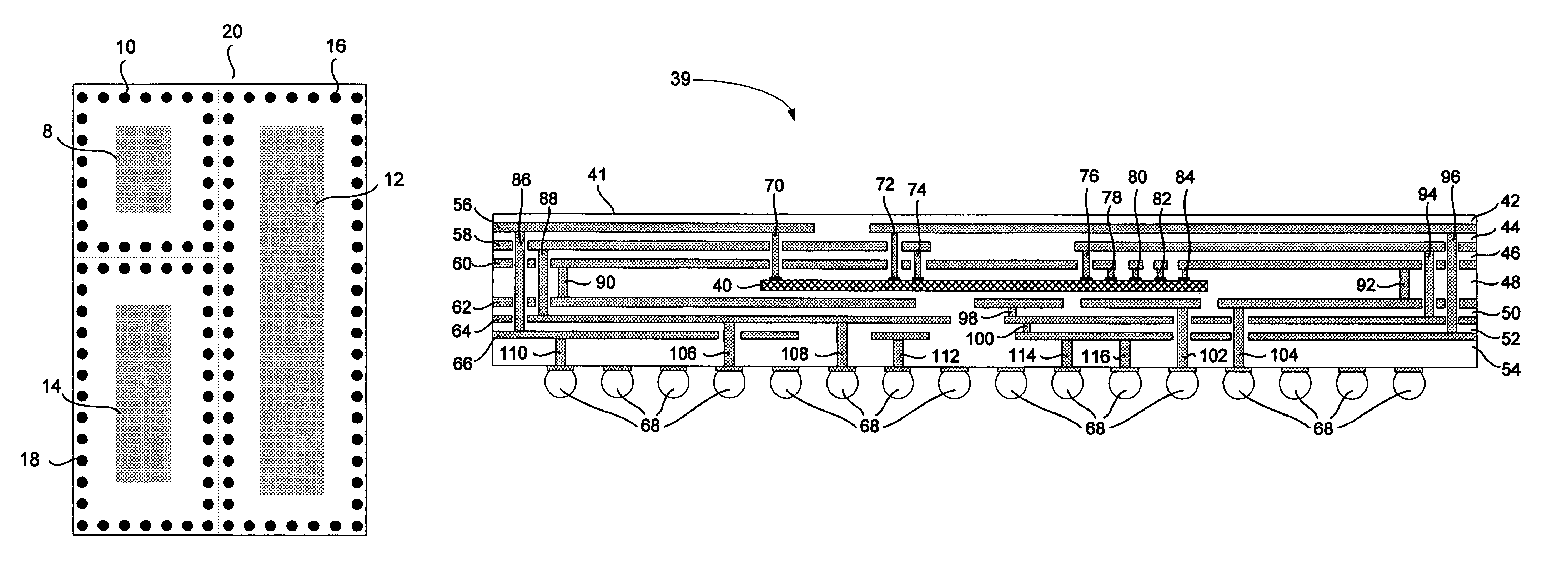
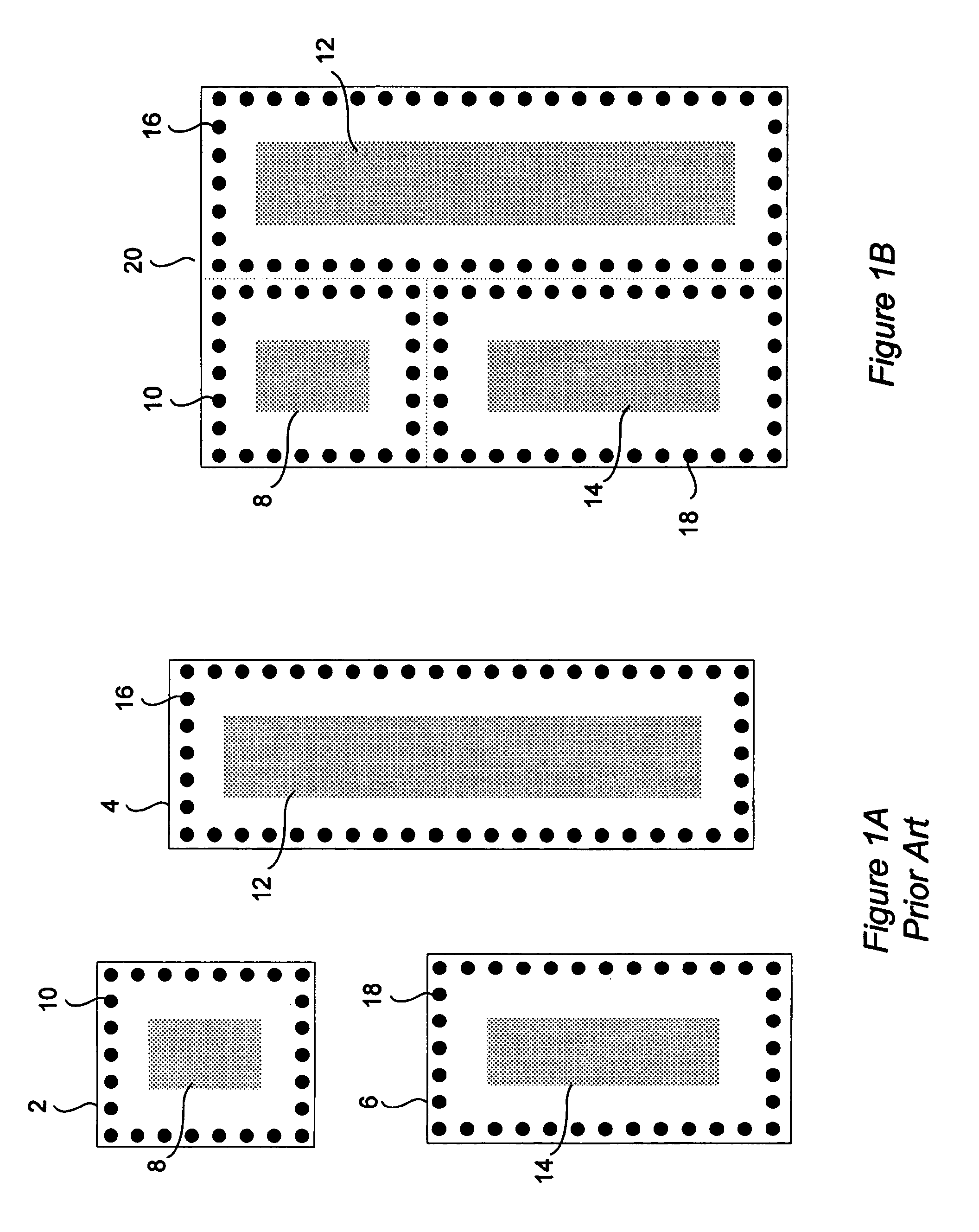
[0028]In the first embodiment, the first, second and third dice 2, 4, 6 have dimensions such that, when they are placed on the combination die 20 with no rearrangement of the die connectors 10, 16, 18, the total area of the combination die 20 is equal to the sum of the areas of the first, second and third dice 2, 4, 6.
second embodiment
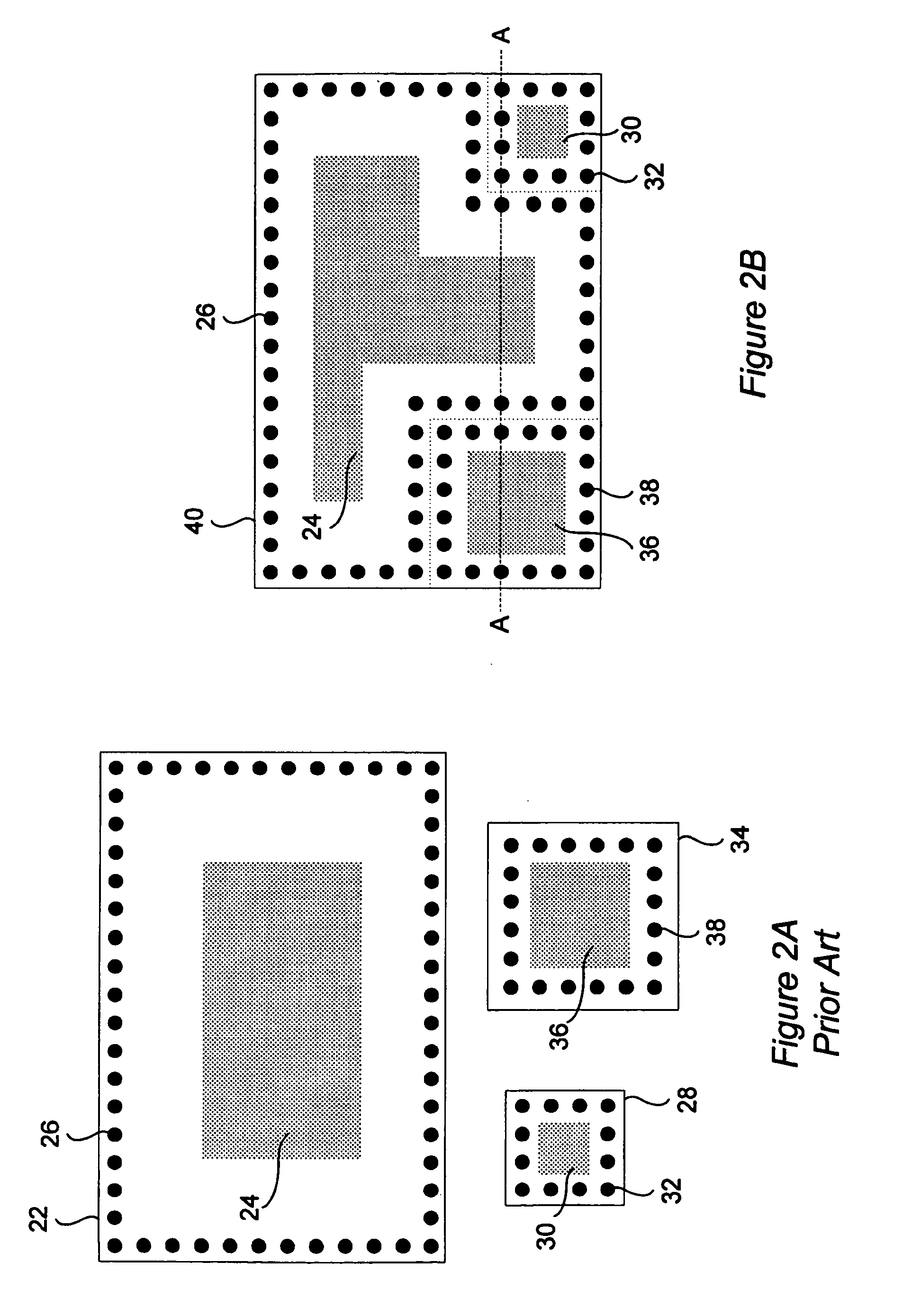
[0029]In a second embodiment, which will now be described with reference to FIGS. 2A and 2B, the dimensions of a combination die, comprising functional blocks and connectors in the same relative positions to one another as on their single-function dice, may be slightly less than the sum of the areas of the individual die.
[0030]FIG. 2A shows three single-function dice 22, 28, 34. These single-function die have the same general structure as the first, second and third die 2, 4, 6, of FIG. 1A, although they have different dimensions and different functionality. Each die 22, 28, 34 is provided with a functional block in its centre 24, 30, 36 and die connectors around its periphery 26, 32, 38.
[0031]As is evident from the dimensions of the single-function dice 22, 28, 34, if a rectangular combination die is created using the functional blocks 24, 30, 36 and die connectors 26, 32, 38 in the same positions relative to one another as on the single-function dice, the area of the combination d...
PUM
 Abstract
Description
Claims
Application Information