Method and apparatus for a semiconductor device with a high-k gate dielectric

a technology of high-k dielectric and semiconductor devices, applied in the direction of electrical apparatus, semiconductor devices, basic electric elements, etc., can solve the problems of gate dielectric leakage, short channel effect (sce), and less desirable commercial devices using high-k dielectric materials

Active Publication Date: 2008-02-19
TAIWAN SEMICON MFG CO LTD
View PDF34 Cites 22 Cited by
  • Summary
  • Abstract
  • Description
  • Claims
  • Application Information

AI Technical Summary

Benefits of technology

[0010]Various embodiments of the present invention provide a novel process and structure for a planar MOS transistor using a high-k gate dielectric material. In a first preferred embodiment of the structure of the invention, a high-k dielectric is provided over a substrate, a gate electrode material is deposited over the high-k dielectric, a protective mask is deposited over the electrode, this mask is patterned, and the gate electrode and gate dielectric structure are subsequently completed by an anisotropic etch which extends through the dielectric layer and into the underlying substrate material beneath the bottom of the dielectric material. The resulting structure is then processed further to include sidewall spacers and self-aligned source and drain regions to form complete MOS transistors, the sidewall spacers covering the sides of the gate electrodes including the portion of the area beneath the bottom of the dielectric layer. Because the sidewall covering extends beneath the channel dielectric interface area, the possibility is reduced that undesirable intrusion of material, including oxygen or hydrogen atoms, will infiltrate any of the channel region, the interface between the substrate channel and the dielectric, the dielectric, or the interface between the dielectric material and the gate electrode material. The high-k dielectric in the resulting MOS transistor devices thus remains its electrical property with desirable dielectric constant (k).
[0011]In a preferred embodiment, a counter-doped channel is created in the substrate in the regions where the transistors will be formed by using conventional ion implantation into the substrate. The counter-doped channel increases performance and adds additional advantages such as allowing the adjustment of voltage thresholds, Vt, for the completed transistors.
[0012]In a preferred embodiment, a channel material of, for example, strained silicon (Si) or strained silicon germanium (SiGe) or their combination is deposited beneath the dielectric material to provide the channel for the resulting devices and to increase the carrier mobility with reduced threshold voltage; optionally this channel material may be counter-doped to further provide enhanced transistor performance. Again the sidewall spacers extend into this layer and extend beneath the bottom of the high-k dielectric layer to prevent undesirable impurities, including oxygen or hydrogen atoms, from infiltrating the structure and from degrading the high-k dielectric.
[0015]In another preferred embodiment, the strained channel layer may be counter-doped to enhance transistor performance and provide further Vt control. Using photomasks to form resist, some or all of the transistors may be subjected to the counter-doping, or some may not be counter-doped.
[0017]In another preferred embodiment, a metal gate electrode or a combination material including a metal may be used for the gate electrode, for example a TiN (Titanium Nitride) metal gate electrode may be used. Polysilicon, and doped polysilicon, may be used for the gate electrode, the polysilicon gate electrodes may also incorporate an additional salicide coating for better performance.
[0018]In another preferred embodiment, the channel material is deposited over the substrate, a gate dielectric and gate electrode material is provided over the substrate and the channel material, a photomask patterning and etch is performed to form the gate electrodes and dielectrics having sidewalls extending into the channel material, sidewall spacers are formed on the sidewalls of the gate electrodes and dielectrics and extending beneath the bottom of the gate dielectric material, and a subsequent etch is performed to remove any of the remaining channel material completely outside of those areas under the completed gate electrodes to reveal the silicon or other substrate prior to subsequent processing. Again the sidewall oxides extend to a depth beneath the gate dielectric and protect the strained channel material from undesirable infiltrations of materials including oxygen (O) and hydrogen (H), which might otherwise form unwanted compounds including oxides in the counter-doping channel material and relax the strained material, reducing its effectiveness.

Problems solved by technology

Reduced device scaling with conventional gate dielectrics creates problems in manufacturing reliable MOS transistors, including short channel effects (SCE) and gate dielectric leakage.
The use of such materials creates additional problems, however, in the manufacturing and reliability of the transistor devices, including a threshold voltage (Vt) variability in the MOS transistors, particularly of p-type MOS transistors, which makes commercial devices using the high-k dielectric materials less desirable.
Further, reduction in scale and the use of certain desirable high-k dielectric materials on silicon substrates are believed to contribute to a reported degradation in carrier mobility, which has a negative effect on the performance of transistors, manufactured using these materials.

Method used


Image

  • Method and apparatus for a semiconductor device with a high-k gate dielectric
  • Method and apparatus for a semiconductor device with a high-k gate dielectric
  • Method and apparatus for a semiconductor device with a high-k gate dielectric

Examples


Embodiment Construction

[0038]The operation and fabrication of the presently preferred embodiments are discussed in detail below. However, the embodiments and examples described herein are not the only applications or uses contemplated for the invention. The specific embodiments discussed are merely illustrative of specific ways to make and use the invention, and do not limit the scope of the invention or the appended claims.

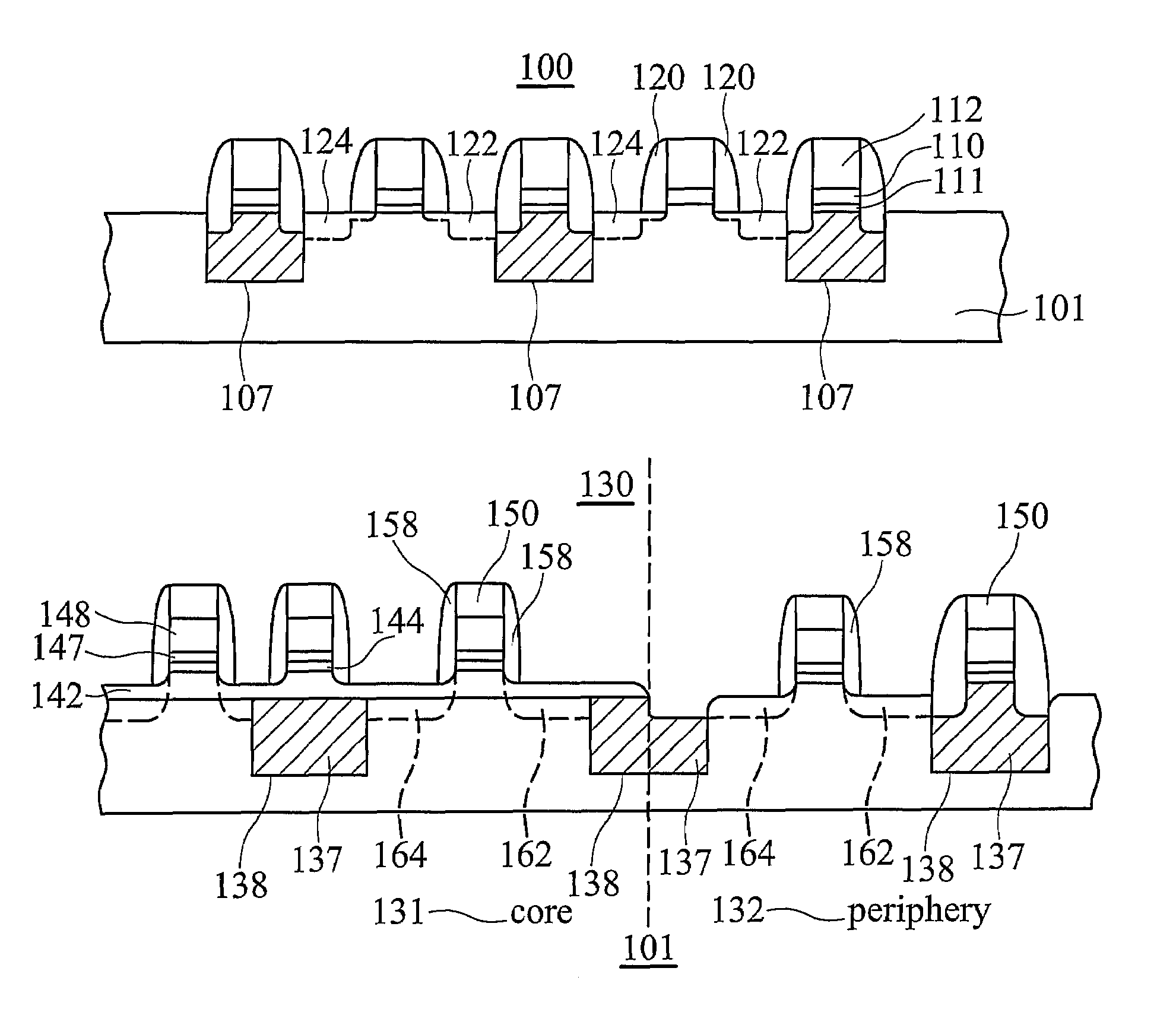
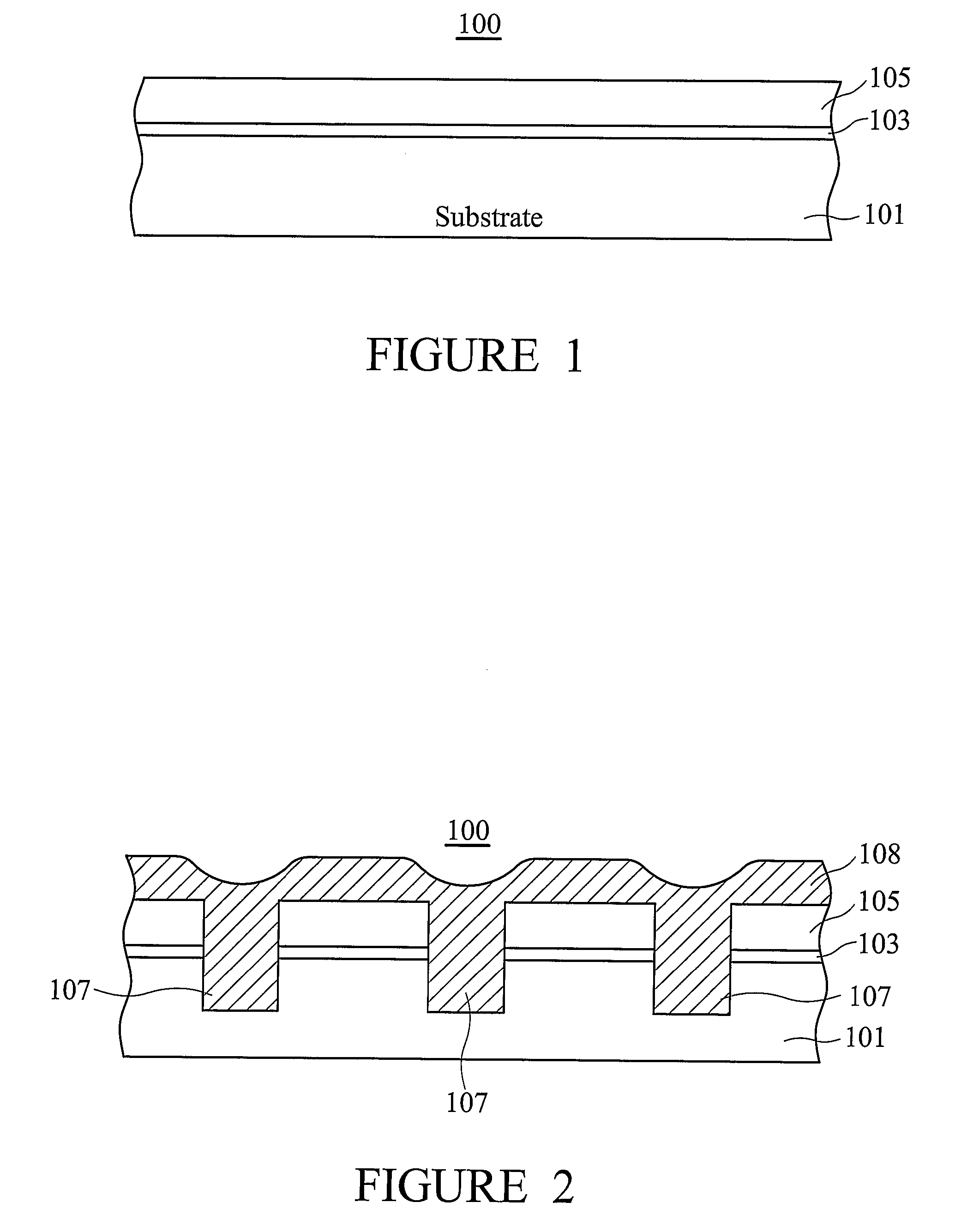
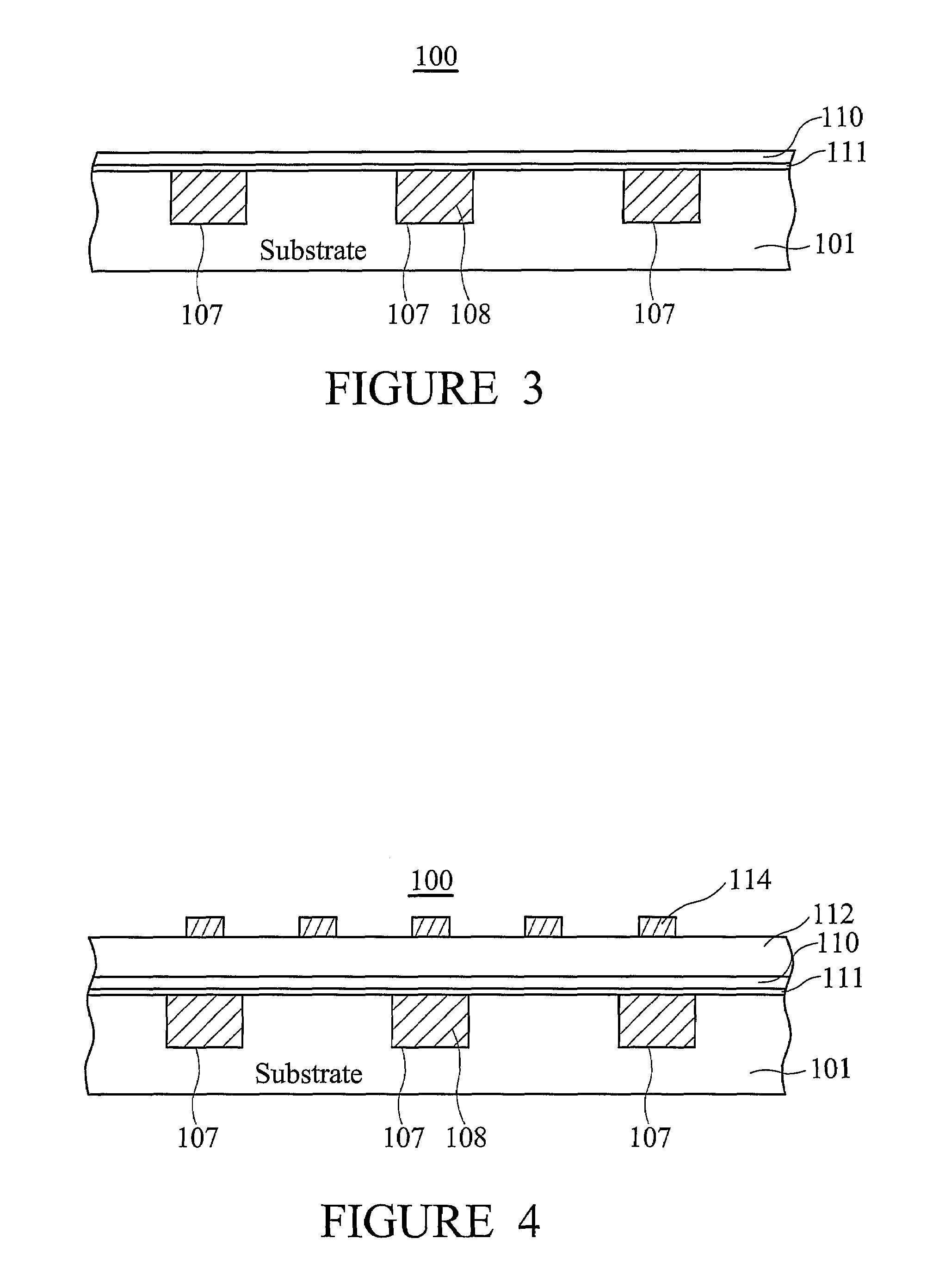
[0039]FIG. 1 depicts a cross sectional view of an integrated circuit 100 not drawn to scale, but drawn as an illustration only. Semiconductor substrate 101 will provide the basic material for the manufacture of the circuit. Substrate 101 is shown with a pad oxide layer 103 and a nitride layer 105 deposited over it using typical deposition processes, for example the depositions may be a chemical vapor deposition, a plasma enhanced deposition, or any other blanket deposition known in the art, such as reduced pressure CVD or others. The nitride layer 105 can be formed by LPCVD with a resu...


PUM


Abstract

A process and apparatus for a high-k gate dielectric MOS transistor is described. A substrate is provided, a high-k gate dielectric material is deposited over the substrate, a gate electrode layer is deposited over the dielectric material and a patterning step is performed creating sidewalls of the electrode and dielectric and removing a portion of the substrate. Sidewall material is deposited over the patterned gate electrode and dielectric creating protective sidewalls on the patterned gate electrode and dielectric that extend beneath the bottom of the dielectric. In alternative embodiments a channel material is deposited beneath the high-k gate dielectric and the patterning step removes at least a portion of the channel material beneath the high-k gate dielectric. In alternative embodiments the channel material is counter-doped.

Description

CROSS-REFERENCE TO RELATED APPLICATIONS[0001]This application is related to co-pending and commonly assigned U.S. application Ser. No. 11 / 185,443, filed Jul. 20, 2005, which application is incorporated herein by reference.[0002]This application is a continuation application of U.S. application Ser. No. 11 / 021,269, filed on Dec. 23, 2004 now U.S. Pat. No. 7,229,893, entitled “Method and Apparatus for a Semiconductor Device with a High-k Gate Dielectric,” which application is hereby incorporated herein by reference.TECHNICAL FIELD[0003]The present invention and the various embodiments described generally relate to the fabrication of semiconductor devices, and more particularly to fabricating integrated devices which incorporate at least one planar MOS transistor having a high-k gate dielectric.BACKGROUND[0004]In the semiconductor art, it is desirable to improve transistor performance even as devices become smaller due to ongoing scaling. Reduced device scaling with conventional gate d...

Claims


Application Information

Patent Timeline
Patent Type & Authority Patents(United States)
IPC IPC(8): H01L21/76
CPCH01L21/28123H01L21/28194H01L21/823462H01L21/823468H01L21/823481H01L21/823857H01L21/823864H01L21/823878H01L27/10873H01L27/10894H01L29/517H10B12/05H10B12/09
Inventor WANG, CHIH-HAOTSAI, CHING-WEICHEN, SHANG-CHIH
Owner TAIWAN SEMICON MFG CO LTD
Why Eureka
Try Eureka