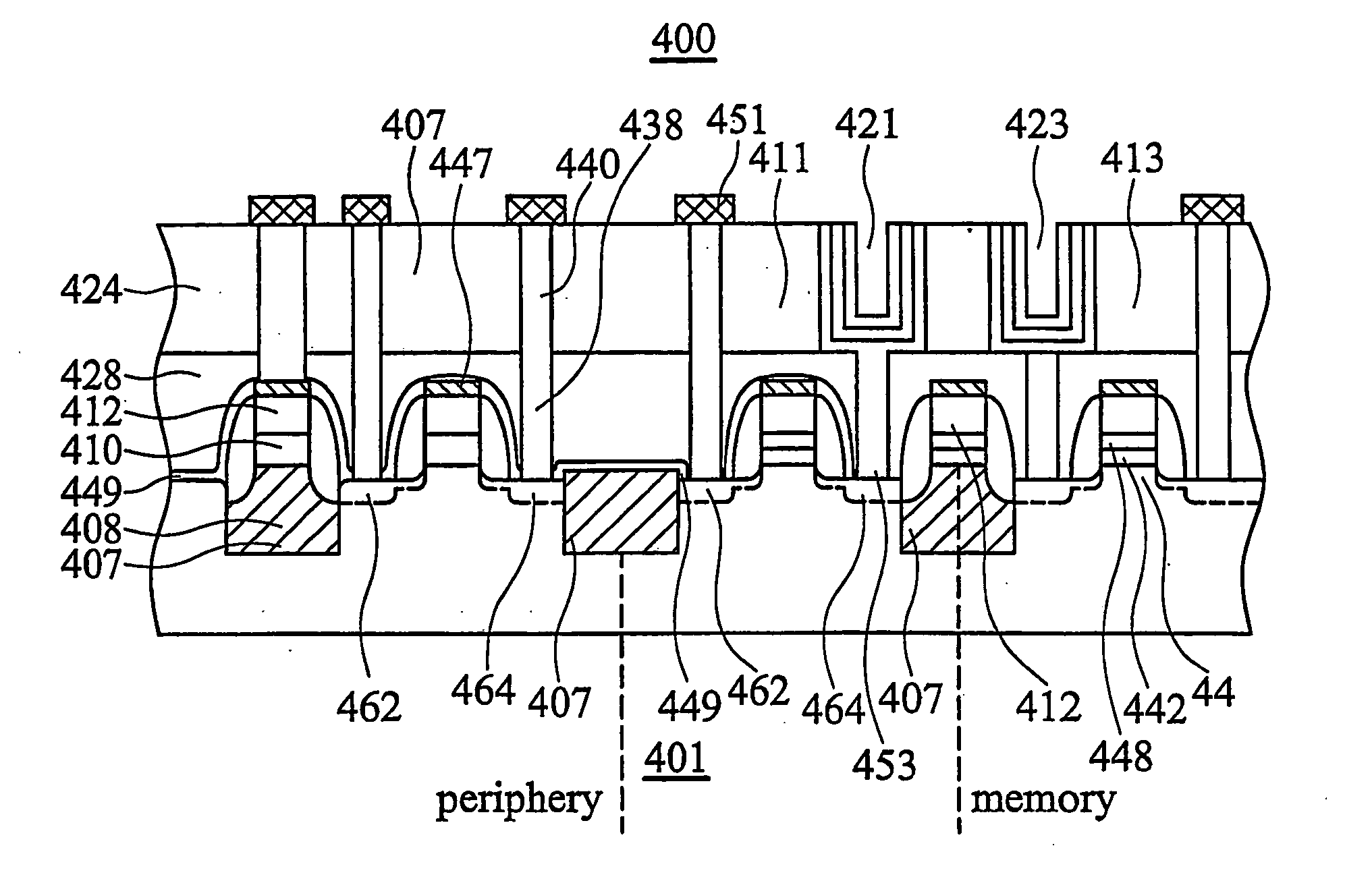
[0010] Various embodiments of the present invention provide a novel process and structure for a planar MOS transistor using a high-k gate dielectric material. In a first preferred embodiment of the structure of the invention, a high-k dielectric is provided over a substrate, a gate
electrode material is deposited over the high-k dielectric, a protective
mask is deposited over the electrode, this
mask is patterned, and the gate electrode
and gate dielectric structure are subsequently completed by an anisotropic etch which extends through the
dielectric layer and into the underlying substrate material beneath the bottom of the dielectric material. The resulting structure is then processed further to include sidewall spacers and self-aligned source and drain regions to form complete MOS transistors, the sidewall spacers covering the sides of the gate electrodes including the portion of the area beneath the bottom of the
dielectric layer. Because the sidewall covering extends beneath the channel dielectric interface area, the possibility is reduced that undesirable intrusion of material, including
oxygen or
hydrogen atoms, will infiltrate any of the channel region, the interface between the substrate channel and the dielectric, the dielectric, or the interface between the dielectric material and the gate
electrode material. The high-k dielectric in the resulting MOS transistor devices thus remains its electrical property with desirable dielectric constant (k).
[0011] In a preferred embodiment, a counter-doped channel is created in the substrate in the regions where the transistors will be formed by using conventional
ion implantation into the substrate. The counter-doped channel increases performance and adds additional advantages such as allowing the adjustment of
voltage thresholds, Vt, for the completed transistors.
[0012] In a preferred embodiment, a channel material of, for example,
strained silicon (Si) or
strained silicon germanium (SiGe) or their combination is deposited beneath the dielectric material to provide the channel for the resulting devices and to increase the carrier mobility with reduced
threshold voltage, optionally this channel material may be counter-doped to further provide enhanced transistor performance. Again the sidewall spacers extend into this layer and extend beneath the bottom of the high-k
dielectric layer to prevent undesirable impurities, including
oxygen or
hydrogen atoms, from infiltrating the structure and from degrading the high-k dielectric.
[0015] In another preferred embodiment, the strained channel layer may be counter-doped to enhance transistor performance and provide further Vt control. Using photomasks to form
resist, some or all of the transistors may be subjected to the counter-
doping, or some may not be counter-doped.
[0017] In another preferred embodiment, a
metal gate electrode or a combination material including a
metal may be used for the gate electrode, for example a-
TiN (
Titanium Nitride)
metal gate electrode may be used. Polysilicon, and doped polysilicon, may be used for the gate electrode, the
polysilicon gate electrodes may also incorporate an additional
salicide coating for better performance.
[0018] In another preferred embodiment, the channel material is deposited over the substrate, a gate dielectric
and gate electrode material is provided over the substrate and the channel material, a
photomask patterning and etch is performed to form the gate electrodes and dielectrics having sidewalls extending into the channel material, sidewall spacers are formed on the sidewalls of the gate electrodes and dielectrics and extending beneath the bottom of the gate dielectric material, and a subsequent etch is performed to remove any of the remaining channel material completely outside of those areas under the completed gate electrodes to reveal the
silicon or other substrate prior to subsequent
processing. Again the sidewall oxides extend to a depth beneath the gate dielectric and protect the strained channel material from undesirable infiltrations of materials including
oxygen (O) and
hydrogen (H), which might otherwise form unwanted compounds including oxides in the counter-
doping channel material and relax the strained material, reducing its effectiveness.
