

Circuit board having test coupon and method for evaluating the circuit board
a circuit board and coupon technology, applied in the direction of semiconductor/solid-state device testing/measurement, circuit inspection/indentification, semiconductor/solid-state device details, etc., can solve the problems of difficult to determine whether the circuit board having the conductor has good performance and difficult to evaluate the characteristics of the conductor
- Summary
- Abstract
- Description
- Claims
- Application Information
AI Technical Summary
Benefits of technology
Problems solved by technology
Method used
Image

Examples
first embodiment
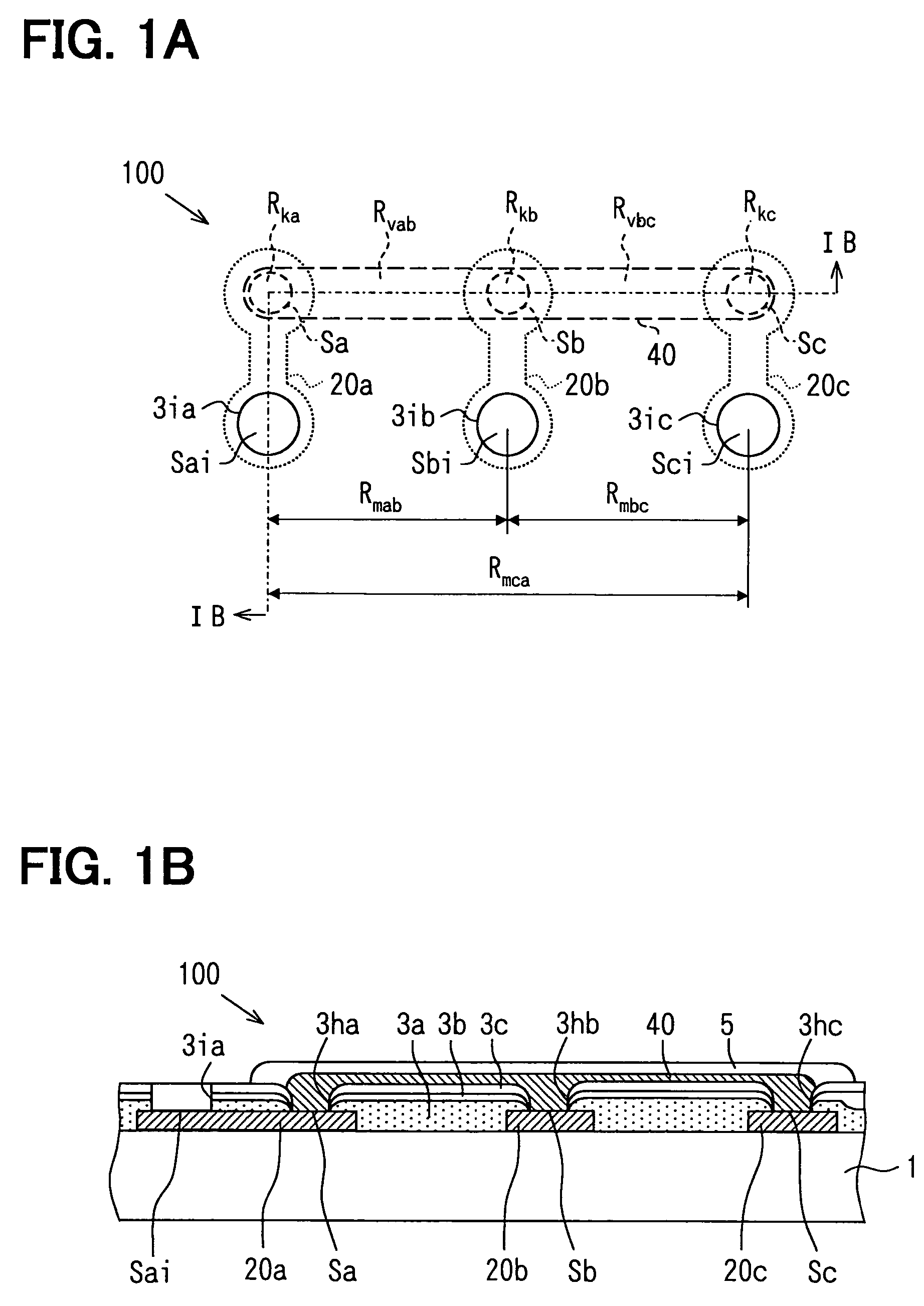
[0029]The inventors have preliminarily studied about a circuit board as a comparison. The circuit board has a conductive paste layer as a conductor. The circuit board 90 is shown in FIG. 11. The circuit board 90 includes an insulation substrate 1, multiple conductive patterns 2a-2c, lower insulation layers 3a-3c, a conductive paste layer 4, and an upper insulation layer 5.
[0030]The conductive patterns 2a-2c are disposed on the surface of the insulation substrate 1. The lower insulation layers 3a-3c cover the conductive patterns 2a-2c. One of the lower insulation layer 3a is a solder resist layer, and has an opening 3ah so that two conductive patterns 2a, 2c are partially exposed from the lower insulation layer 3a through the opening 3ah. The other two lower insulation layers 3b, 3c provide a double layered under coat layer, which insulates the conductive pattern 2b from the other two conductive patterns 2a, 2c. The conductive paste layer 4 is formed on the lower insulation layers 3a...
second embodiment
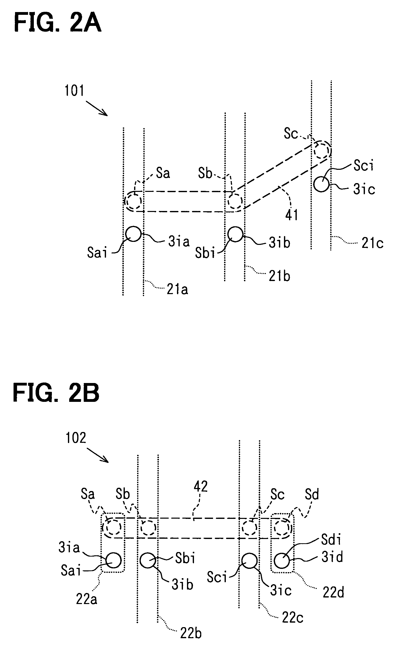
[0050]Circuit boards 101, 102 according to a second embodiment of the present invention are shown in FIGS. 2A and 2B.
[0051]FIG. 2A shows the circuit board 101 including three lower conductive patterns 21a-21c before an electric device is mounted on the circuit board 101. The lower conductive patterns 21a-21c are not connected together except for the connection portions Sa-Sc so that each lower conductive pattern 21a-21c is independent each other. A conductive paste layer 41 as an upper conductive layer connects to each lower conductive pattern 21a-21c at a connection portion Sa-Sc through the interlayer insulation layer 3a-3c (not shown). Accordingly, the conductive paste layer 41 becomes a jumper wire for connecting among the three lower conductive patterns 21a-21c. Each lower conductive pattern 21a-21c exposed through the opening 3ia-3ic works as the resistance check land Sai-Sci corresponding to the connection portion Sa-Sc.
[0052]In the circuit board 101, the boundary resistance ...
third embodiment
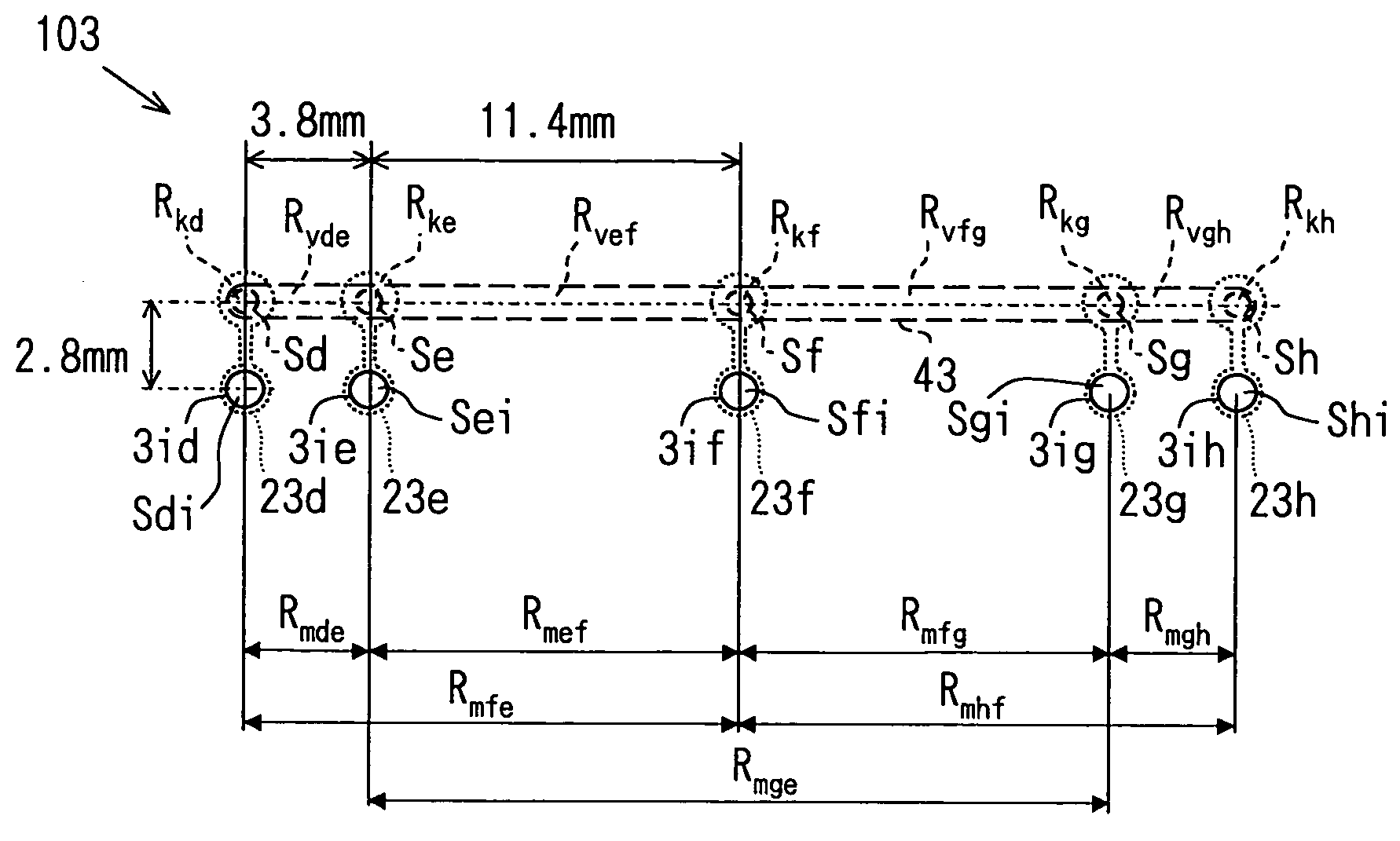
[0058]A circuit board 103 according to a third embodiment of the present invention is shown in FIG. 3. In the circuit board 103, an independent conductive paste layer 43 as the upper conductive layer connects to each of five lower conductive patterns 23d-23h at the connection portion Sd-Sh. The lower conductive pattern 23d-23h exposed through an opening 3id-3ih works as the resistance check land Sdi-Shi corresponding to the connection portion Sd-Sh.
[0059]Although only the boundary resistance Rkb at the connection portion Sb between the lower conductive pattern 20b and the conductive paste layer 40 is obtained in the circuit board 100, not only the boundary resistances Rke-Rkg at the middle connection portions Se-Sg between the lower conductive pattern 23e-23g and the conductive paste layer 43 but also the resistance of the conductive paste layer 43 itself are obtained at the same time in the circuit board 103. The boundary resistances Rke-Rkg and the resistance of the conductive pas...
PUM
 Abstract
Description
Claims
Application Information