Correction of pixels in an organic EL display device

Active Publication Date: 2008-03-18
GLOBAL OLED TECH
View PDF8 Cites 37 Cited by
  • Summary
  • Abstract
  • Description
  • Claims
  • Application Information

AI Technical Summary

Benefits of technology

[0010]It is therefore an object of the present invention to efficiently perform brightness correction. This object is achieved by an organic

Problems solved by technology

As a result, the light emission amount with respect to the data signal (input voltage) is non-uniform for each pixel, so that brightness unevenness occurs.
However, in the method of this patent publication 1, there are problems in that brightness me

Method used


Image

  • Correction of pixels in an organic EL display device
  • Correction of pixels in an organic EL display device
  • Correction of pixels in an organic EL display device

Examples


Example

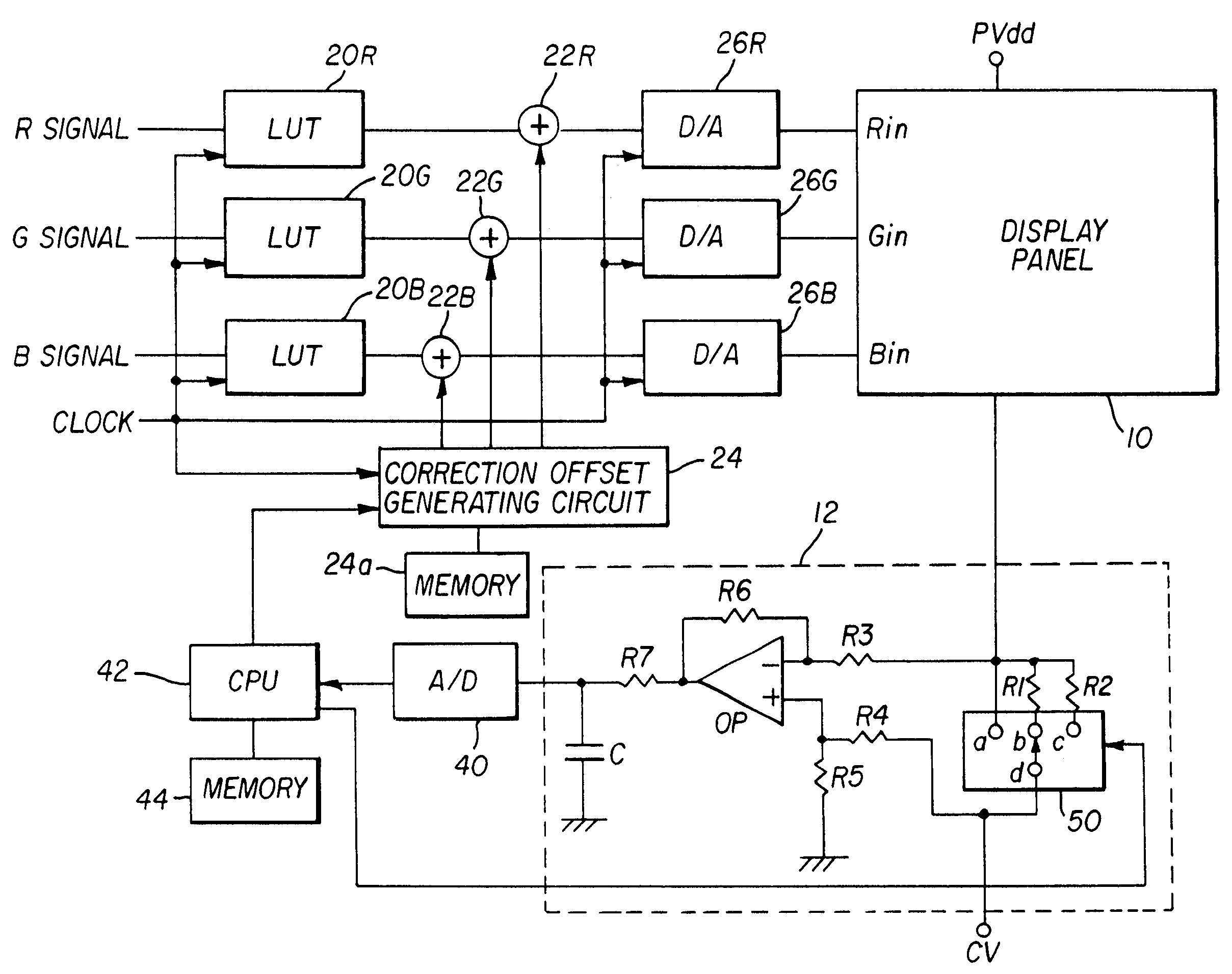
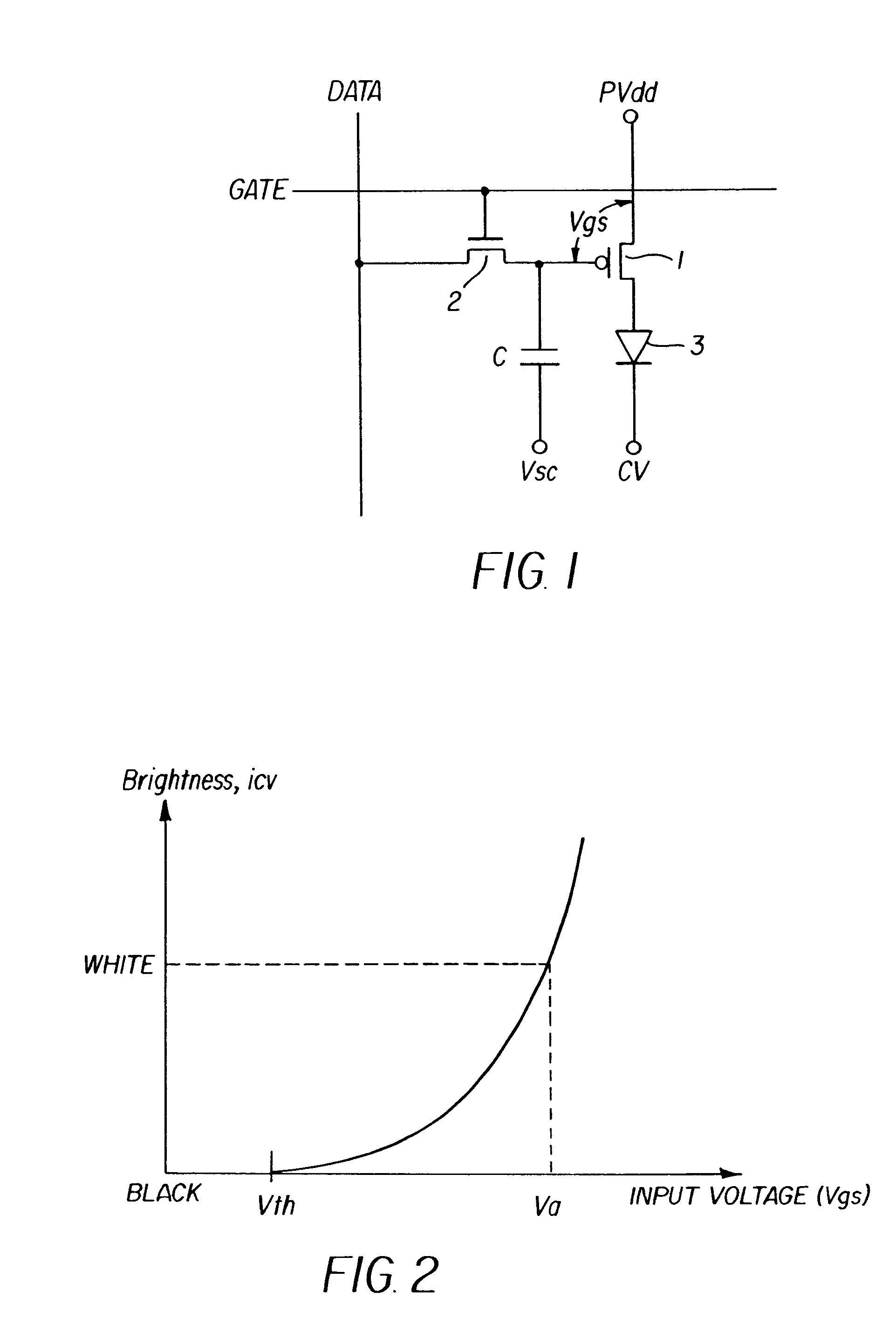
[0035]A display panel is formed on a standard glass substrate, pixel circuits are arranged in matrix form on a display area, and driving circuits are arranged around the periphery thereof. The pixel circuits are produced, for example, by fabricating TFTs and wiring and the like on a glass substrate by a standard technique for fabricating semiconductor integrated circuits, and then forming pixel electrodes such as ITOs, and laminating an organic layer and cathode on top.

[0036]In the case where the display panel is manufactured as described above, a power source is connected, and the total current icv flowing in the organic EL element is measured. That is, as shown in FIG. 4, a power source voltage PVdd is supplied to respective power source lines PVdd of a display panel 10, and a total current Icv which a power source CV causes to flow from a common cathode to all the organic EL elements is measured by a current detector 12, and a correction value formula is produced as described her...


PUM


Abstract

An organic electroluminescent display device in which display pixels containing organic electroluminescent elements are arranged in a matrix, comprising:
    • a correction value formula storage section for storing a correction value formula or coefficients thereof that prescribes a relationship of pixel positions for display and brightness correction data of those pixels;
    • a correction value output section for receiving the input of data for the positions of respective pixels, and outputs correction values for the respective pixels using the correction value formula or coefficients thereof stored in said correction value formula storage section; and
    • the correction value output section corrects brightness data for each pixel using the correction value from said correction value output section according to the pixel position, to thereby perform display to the respective display pixels.

Description

FIELD OF THE INVENTION[0001]The present invention relates to an organic EL (electroluminescent) display device formed by arranging organic EL elements or pixels in matrix form, and more particularly to non-uniformity correction of the elements or pixels.BACKGROUND OF THE INVENTION[0002]FIG. 1 shows a configuration example of a circuit (pixel circuit) for driving one pixel of an active type organic EL display device. A drain of a p-channel driving TFT 1 with a source connected to a source line PVdd is connected to an anode of an organic EL element 3, and a cathode of the organic EL element 3 is connected to a cathode source CV. A source of an n-channel selection TFT 2 is connected to a gate of the driving TFT 1, a drain of this selection TFT 2 is connected to a data line Data, and a gate is connected to a gate line Gate. Furthermore, one end of a holding capacitor C is connected to a gate of the driving TFT 1, and the other end is connected to a capacitor power source line Vsc.[0003]...

Claims


Application Information

Patent Timeline
IPC IPC(8): G09G3/30H05B33/10G09G3/20G09G3/32H01L51/50
CPCG09G3/3233G09G2300/0842G09G2320/0223G09G2320/0233G09G2320/0285G09G2320/029G09G2320/043G09G2320/0626
Inventor MIZUKOSHI, SEIICHIMORI, NOBUYUKIONOMURA, KOUICHIKOHNO, MAKOTO
Owner GLOBAL OLED TECH
Why Eureka
Try Eureka