Intelligent textile technology based on flexible semiconductor skins

a textile technology and flexible technology, applied in weaving, semiconductor/solid-state device details, chemistry apparatus and processes, etc., can solve the problems of increasing the weight and volume of textiles, reducing the flexibility of textiles, and discomforting users

Active Publication Date: 2008-03-25
WAYNE STATE UNIV
View PDF3 Cites 24 Cited by
  • Summary
  • Abstract
  • Description
  • Claims
  • Application Information

AI Technical Summary

Problems solved by technology

However, this methodology suffers from several drawbacks which include a significant decrease in the flexibility of the textiles, discomfort to the user due to the bulkiness of the components, and an increase in the weight and volume of the textiles.
Although this prior art technology is simple and cheap, it too suffers from several drawbacks.
For example, this methodology tends to be temperature limited.
Moreover, such technologies exhibit difficulties in transplanting MEMS devices based on silicon and other rigid materials and in integrating electronics.
Moreover, devices are often stressed when the flexible substrate bends.

Method used


Image

  • Intelligent textile technology based on flexible semiconductor skins
  • Intelligent textile technology based on flexible semiconductor skins
  • Intelligent textile technology based on flexible semiconductor skins

Examples


Embodiment Construction

)

[0015]Reference will now be made in detail to presently preferred compositions or embodiments and methods of the invention, which constitute the best modes of practicing the invention presently known to the inventors.

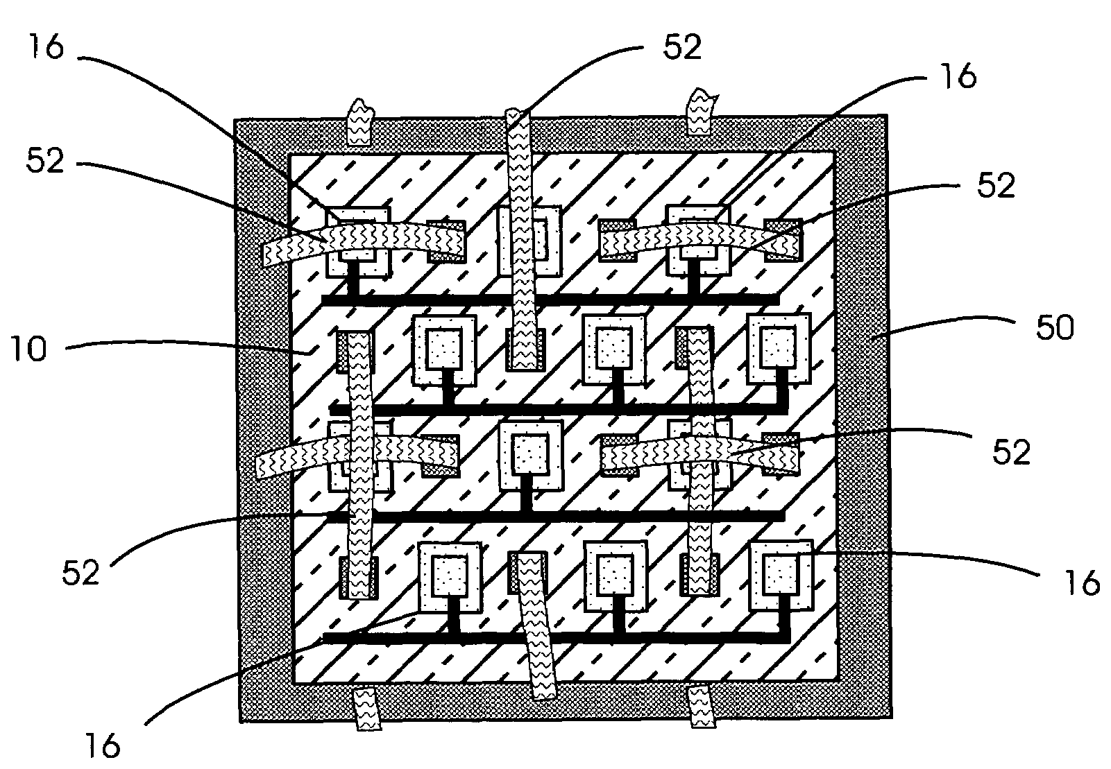
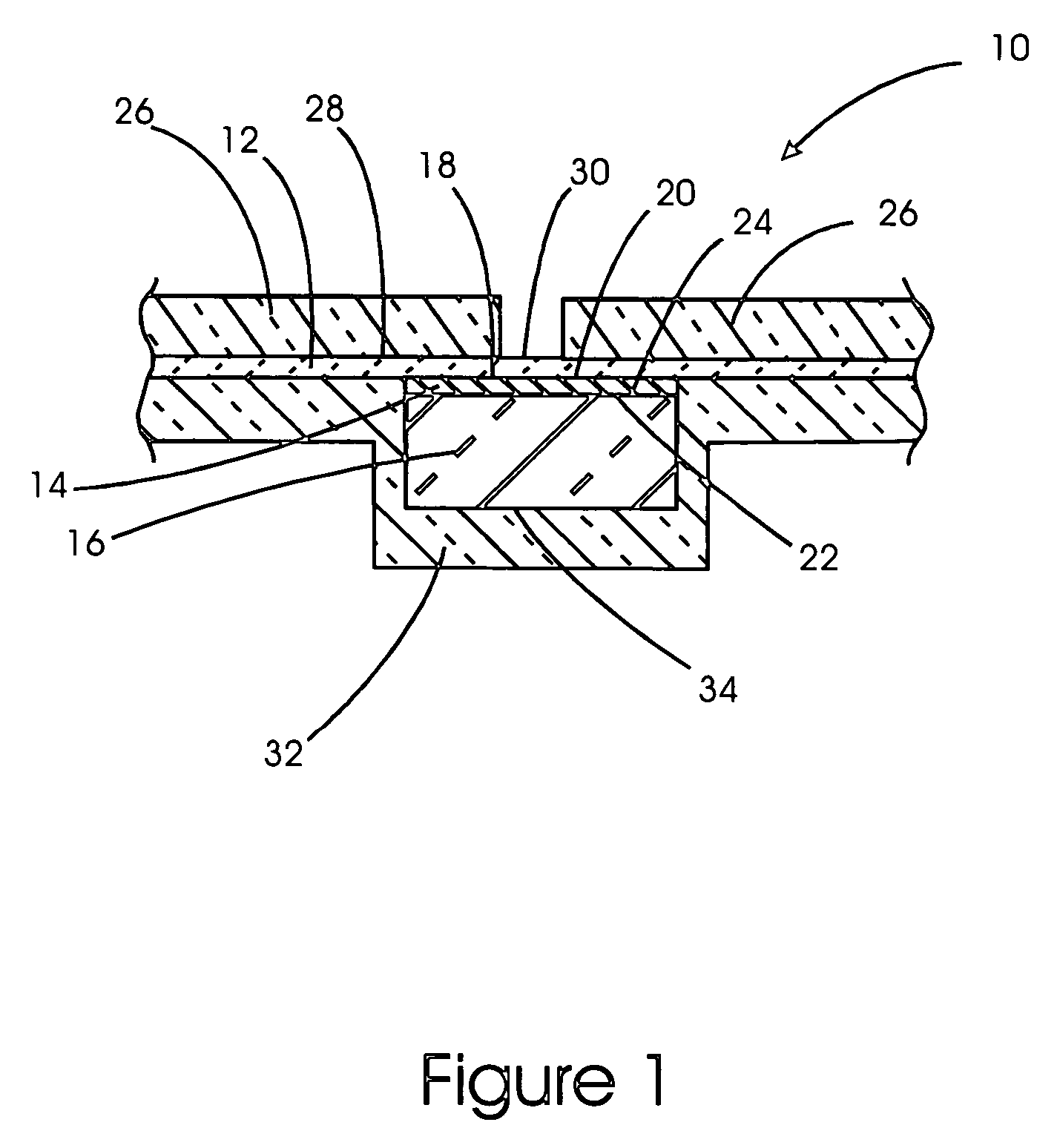
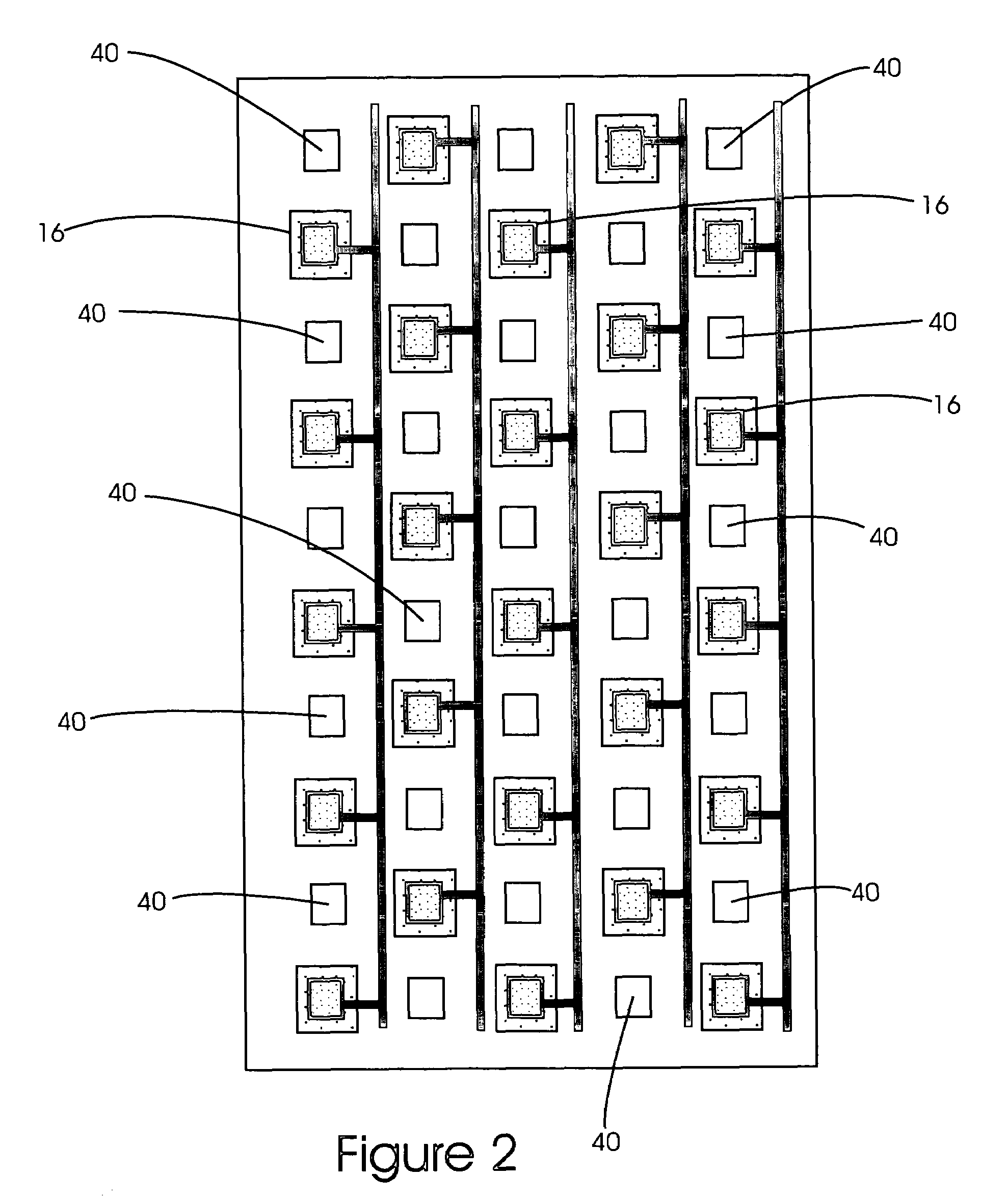
[0016]With reference to FIGS. 1 and 2, an embodiment of the present invention providing a semiconductor-based flexible skin suitable for use in intelligent textile applications is described. Flexible skin 10 includes metal layer 12, insulating layer 14, and one or more semiconductor islands 16. Metal layer 12 is typically patterned into conducting wires that allow electrical communication between the semiconductor islands 16 and to any devices connected to flexible skin 10. Insulating layer 14 is disposed between metal layer 12 and semiconductor islands 16. Specifically, insulating layer 14 is disposed over at least a portion of metal layer 12 such that first metal side 18 is adjacent to first insulating side 20. Similarly, semiconductor islands 16 are disposed over on...


PUM

PropertyMeasurementUnit
flexibleaaaaaaaaaa
semiconductoraaaaaaaaaa
insulatingaaaaaaaaaa

Abstract

A semiconductor-containing flexible skin suitable for use in intelligent textile applications includes a metal layer, an insulating layer, and one or more semiconductor islands sandwiched between a first flexible polymer layer and a second flexible polymer layer. Various electronics and sensors can be advantageously incorporated on the semiconductor islands. The metal layer of the invention is patterned into conducting paths that allow electrical communication between the semiconductor islands and to any devices connected to flexible skin. Moreover, the insulating layer is disposed between the metal layer and semiconductor islands. An intelligent textile includes the semiconductor-containing flexible skin attached to a fabric. Specifically, opening in the flexible textile allow direct weaving with textiles. A method of forming the flexible skin and intelligent fabric is also provided.

Description

BACKGROUND OF THE INVENTION[0001]1. Field of the Invention[0002]The present invention relates to intelligent textile technology based on the integration of semiconductor flexible skins with textiles.[0003]2. Background Art[0004]As semiconductor microfabrication technology has advanced, integrated circuit based devices have been incorporated into a number of non-conventional applications. Examples of microfabrication technology include both standard microelectronic integrated circuit technology and micro-electro-mechanical systems (“MEMS”) technology. Although these two technologies have considerable process overlap, MEMS is generally regarded as pertaining to the integration of mechanical elements, sensors, actuators, and electronics on a silicon substrate exclusive of integrated circuit technology. Although the distinction is somewhat gray, both technologies together provide the ability to create smart systems in which MEMS components allow the collection of information or the mani...

Claims


Application Information

Patent Timeline
Patent Type & Authority Patents(United States)
IPC IPC(8): H01L29/84
CPCB32B15/08D03D1/0088H01L23/5387H01L24/24A41D1/002H01L25/0655H01L2224/24137H01L2924/14H01L2924/00
Inventor XU, YONG
Owner WAYNE STATE UNIV
Why Eureka
Try Eureka