

Non-volatile switching and memory devices using vertical nanotubes
a technology of vertical nanotubes and switching devices, applied in static storage, digital storage, instruments, etc., can solve problems such as switching devices and changes in state of semiconductor-based memory
- Summary
- Abstract
- Description
- Claims
- Application Information
AI Technical Summary
Problems solved by technology
Method used
Image

Examples
first embodiment
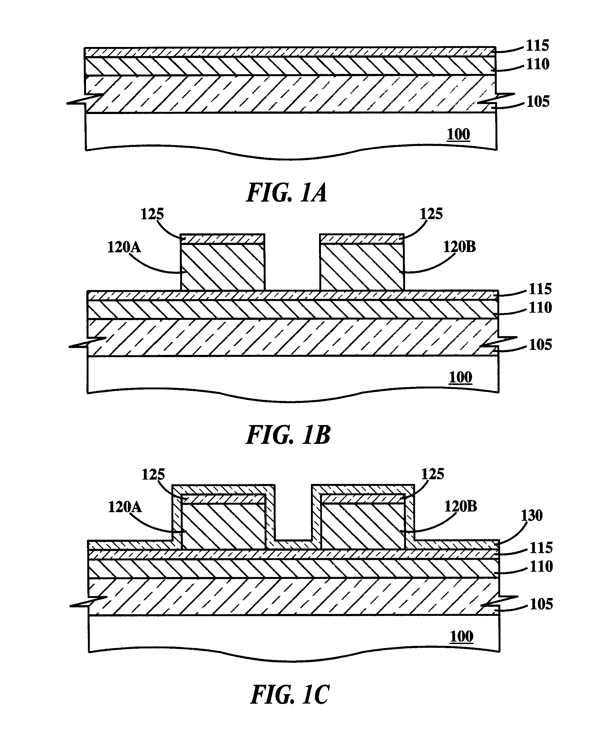
[0030]FIGS. 1A through 1G are cross-sectional views illustrating fabrication of a device according to the present invention. In FIG. 1A, formed on a top surface of a substrate 100 is a first insulating layer 105. The top surface of substrate 100 defines a horizontal plane and a line perpendicular to the top surface of substrate 100 defines a vertical direction. Formed on a top surface of first insulating layer 105 is a bitline 110. Alternatively, bitline 110 may be damascened into first insulating layer 105, top surfaces of the first insulating layer 105 and bitline 110 being coplanar (see FIG. 2). Formed on a top surface of bitline 110 (and exposed top surface of first insulating layer 105) is a first dielectric layer 115.
[0031]In one example, first insulating layer 105 comprises SiO2. In one example, bitline 110 comprises Fe, Co, Ni, other conductive CNT-catalytic material, or combinations thereof. In one example, bitline 110 comprises a layer of Fe, Co, Ni, or other CNT catalytic...
second embodiment
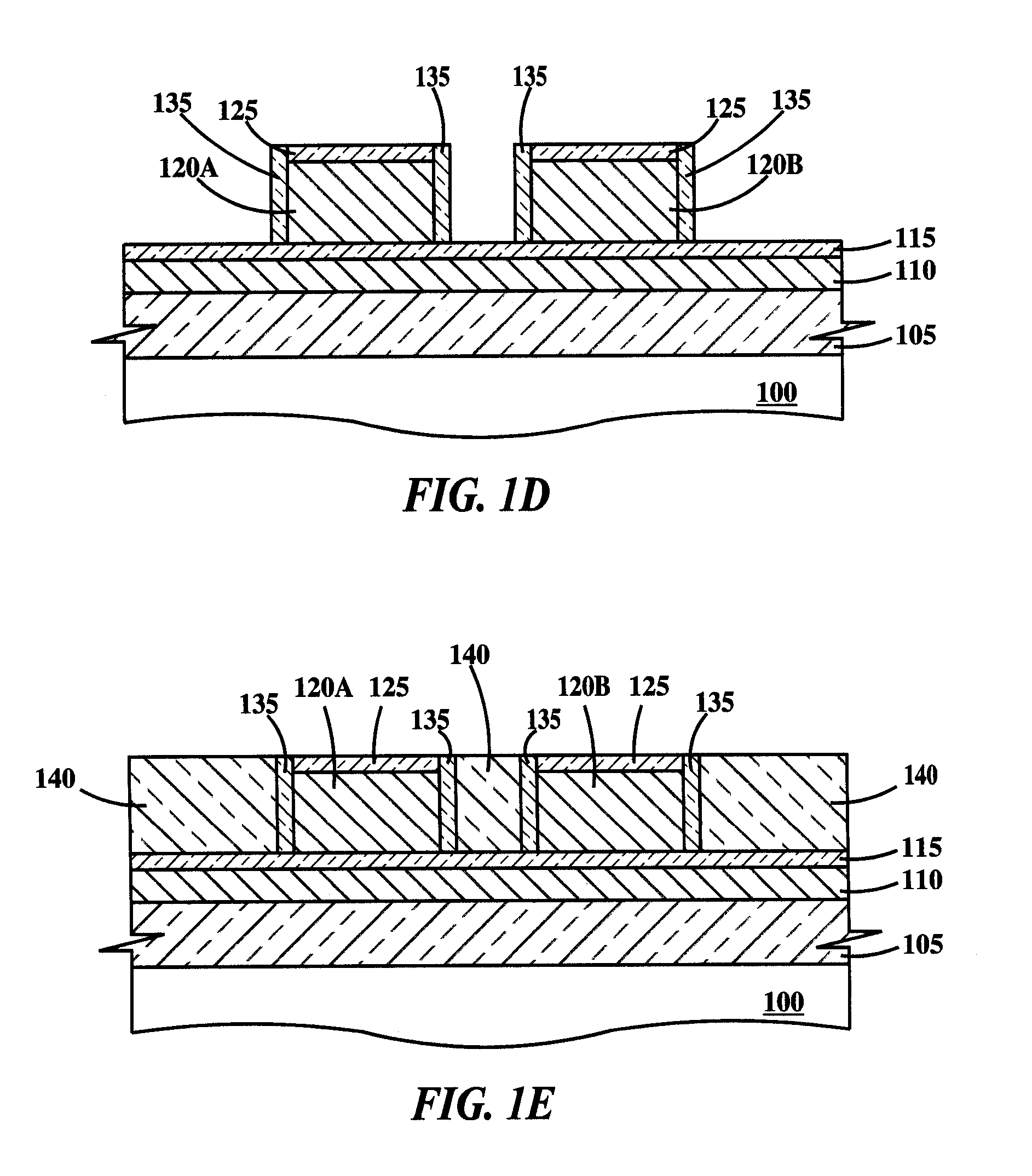
[0051]Bitline 110, wordlines 120A and 120B, dielectric caps 125, dielectric sidewall spacers 135, dielectric spacers 170, and CNTs 155 comprise a switching or memory device (or memory cell) 230 according to the present invention. Substrate 100 may be a semiconductor substrate, for example a bulk silicon or silicon-on-insulator (SOI) substrate, and include devices such as transistors, capacitors, resistors, diodes, and inductors which are wired together to form support circuits for device 230. Operation of device 230 is described infra, in relationship to FIG. 4.
[0052]FIG. 4 is an isometric cross-section of a device according to the second embodiment of the present invention. Change of state of device 230 is similar to that described for device 225 in reference to FIG. 2. However, the method of sensing the state of device 230 is different from that described for device 225 (see FIG. 2). The state (whether CNTs 155 are attached to dielectric spacer 170 on dielectric sidewall spacer 13...
third embodiment
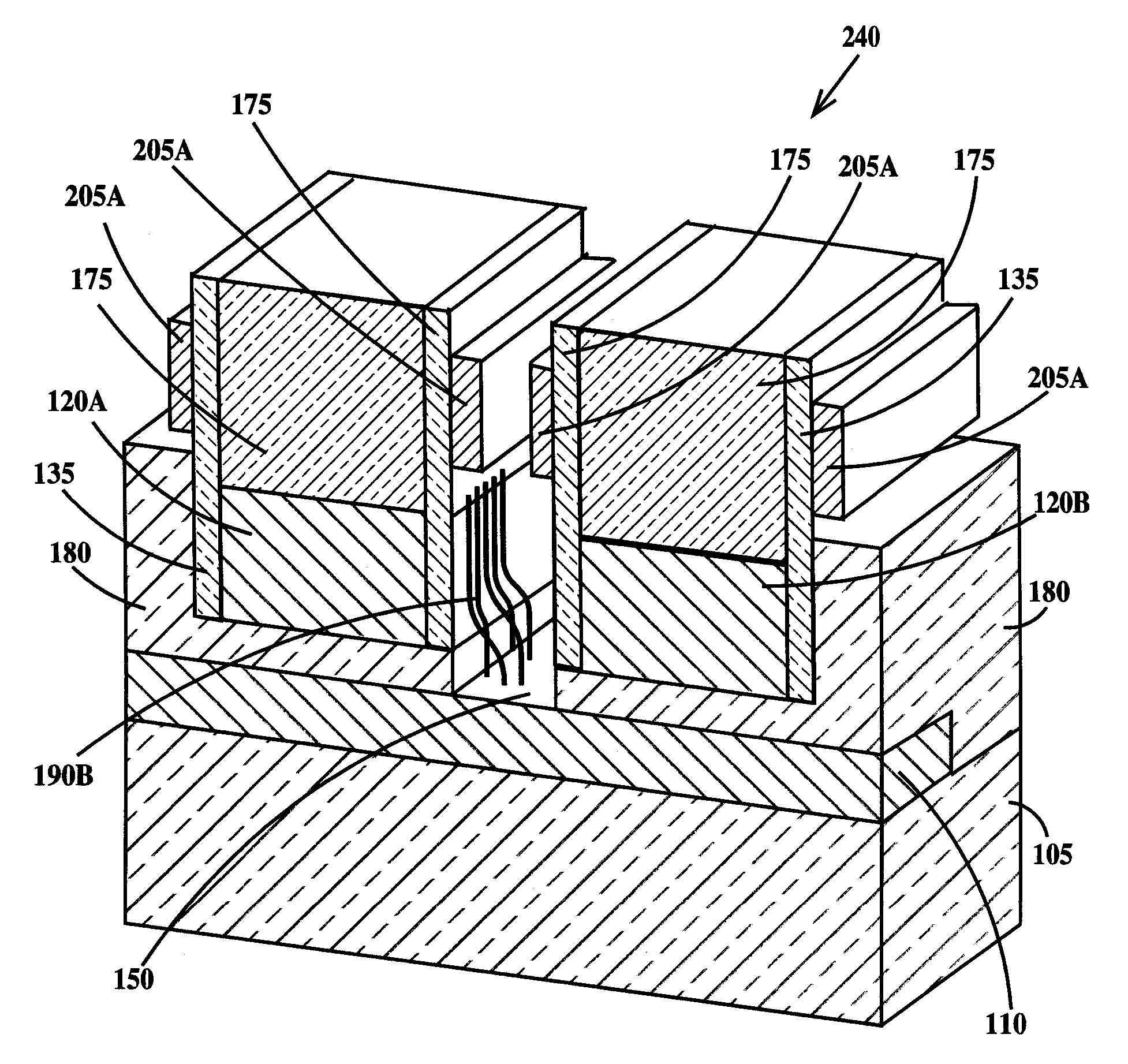
[0065]In FIG. 5K, CNTs 155 are flexible so as to be able to bend and temporally touch dielectric sidewall spacer 135 on first wordline 120A (shown) or touch dielectric sidewall spacer 135 on second wordline 120B. Bitline 110, wordlines 120A and 120B, dielectric sidewall spacers 135, dielectric caps 175, conductive spacers 205A, and CNTs 190B comprise a switching or memory device (or memory cell) 240 according to the present invention. Substrate 100 may be a semiconductor substrate, for example a bulk silicon or silicon-on-insulator (SOI) substrate, and include devices such as transistors, capacitors, resistors, diodes and inductors which are wired together to form support circuits for device 240. Operation of device 240 is described infra, in relationship to FIG. 6.
[0066]FIG. 6 is an isometric cross-section of a device according to the third embodiment of the present invention. Change of state of device 240 is similar to that described supra for device 225 in reference to FIG. 2. Ho...
PUM
 Abstract
Description
Claims
Application Information