Techniques for trimming drive current in output drivers

a technology of output driver and drive current, which is applied in the direction of logic circuit coupling/interface arrangement, pull-up technique, instruments, etc., can solve the problems of reducing the performance or increasing the area of the i/o driver, affecting the actual drive current of the pull-up and pull-down transistors in output drivers, and affecting the performance of the output driver

Inactive Publication Date: 2008-04-08
ALTERA CORP
View PDF10 Cites 20 Cited by
  • Summary
  • Abstract
  • Description
  • Claims
  • Application Information

AI Technical Summary

Problems solved by technology

However, the actual drive current of the pull-up and pull-down transistors in output drivers can differ significantly from design targets, because device models often contain inaccuracies, and the wafer fabrication process varies.
Designing an I / O driver that operates correctly within larger process variations typically involves some compromises that may reduce the performance or increase the area of the I / O driver.
However, building margin into a system may degrade the performance or increase the cost of the system.
Inaccuracies in the models as well as drift in the process can cause the model prediction of a typical output drive current to deviate from the actual drive current observed on silicon.

Method used


Image

  • Techniques for trimming drive current in output drivers
  • Techniques for trimming drive current in output drivers
  • Techniques for trimming drive current in output drivers

Examples


first embodiment

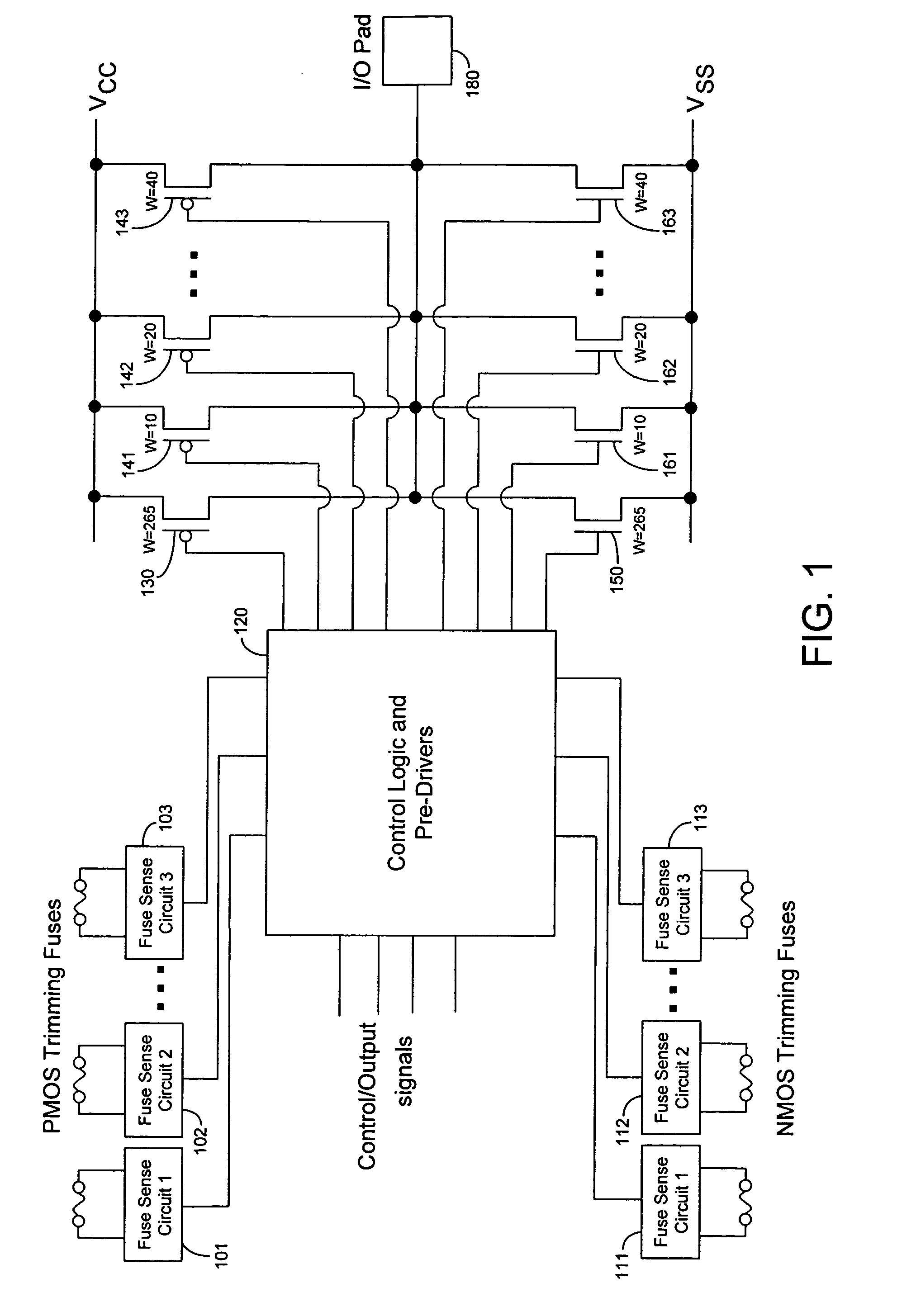
[0022]FIG. 1 illustrates an output driver circuit with an adjustable drive current according to the present invention. FIG. 1 illustrates fuse sense circuits 101-103 and 111-113. Each fuse sense circuit is coupled to a fuse. Only six fuse sense circuits are shown in FIG. 1 so as not to overcomplicate the drawing. It should be understood that any appropriate number of fuse sense circuit can be used to implement embodiment of the present invention.

[0023]Each of the fuse sense circuits controls logic and pre-driver circuit block 120. Each fuse sense circuit is also coupled to a fuse. The fuses can be on-chip fuses or off-chip fuses. The fuses can be, for example, electrical fuses or laser fuses. An electrical fuse can be fabricated on a semiconductor die, for example, on a metal or polysilicon layer. An electrical fuse is blown by driving a large current through the fuse. A laser fuse is blown by a laser. Other types of fuses and methods of storing data can be used as well. For example...

second embodiment

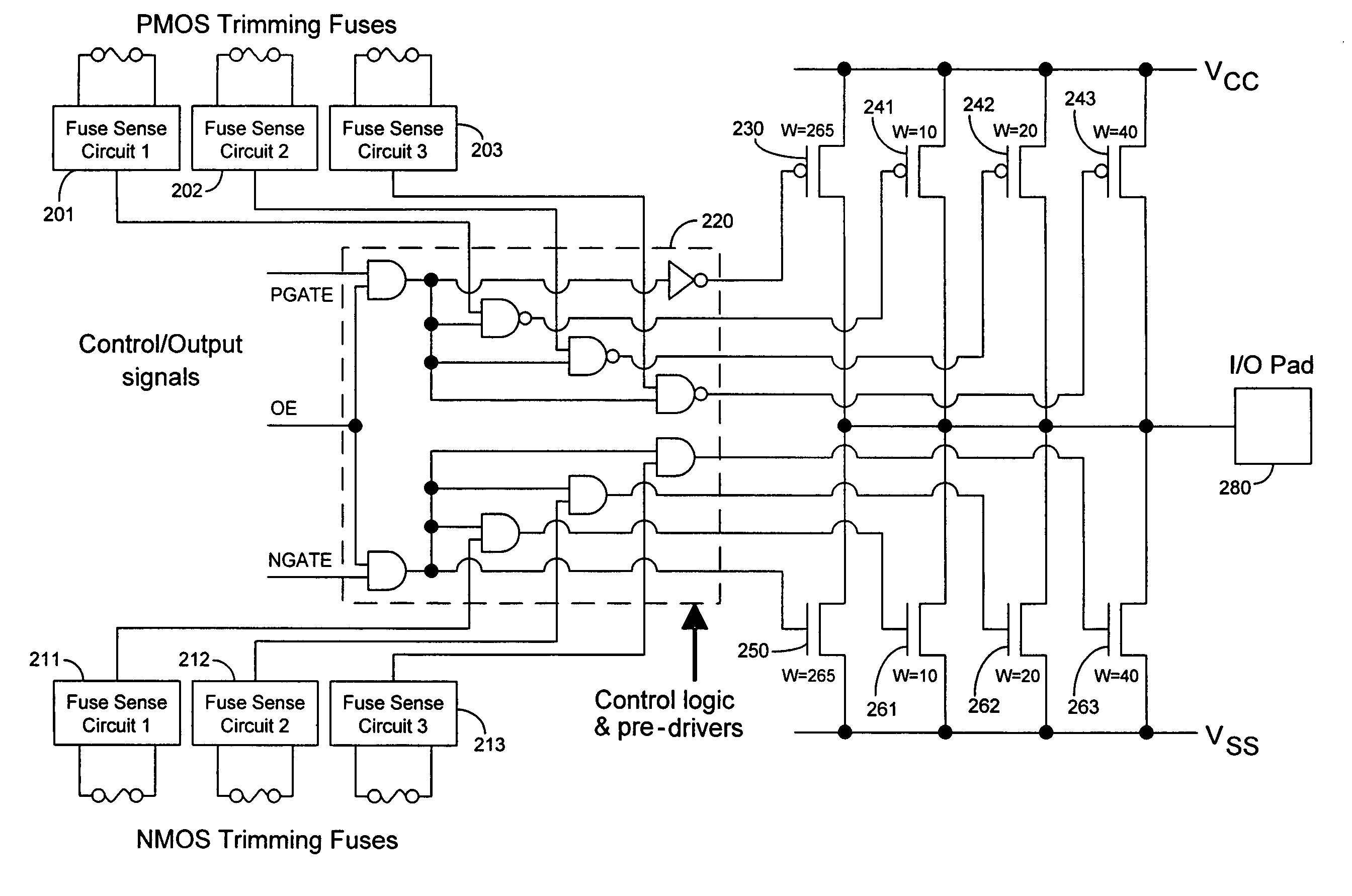
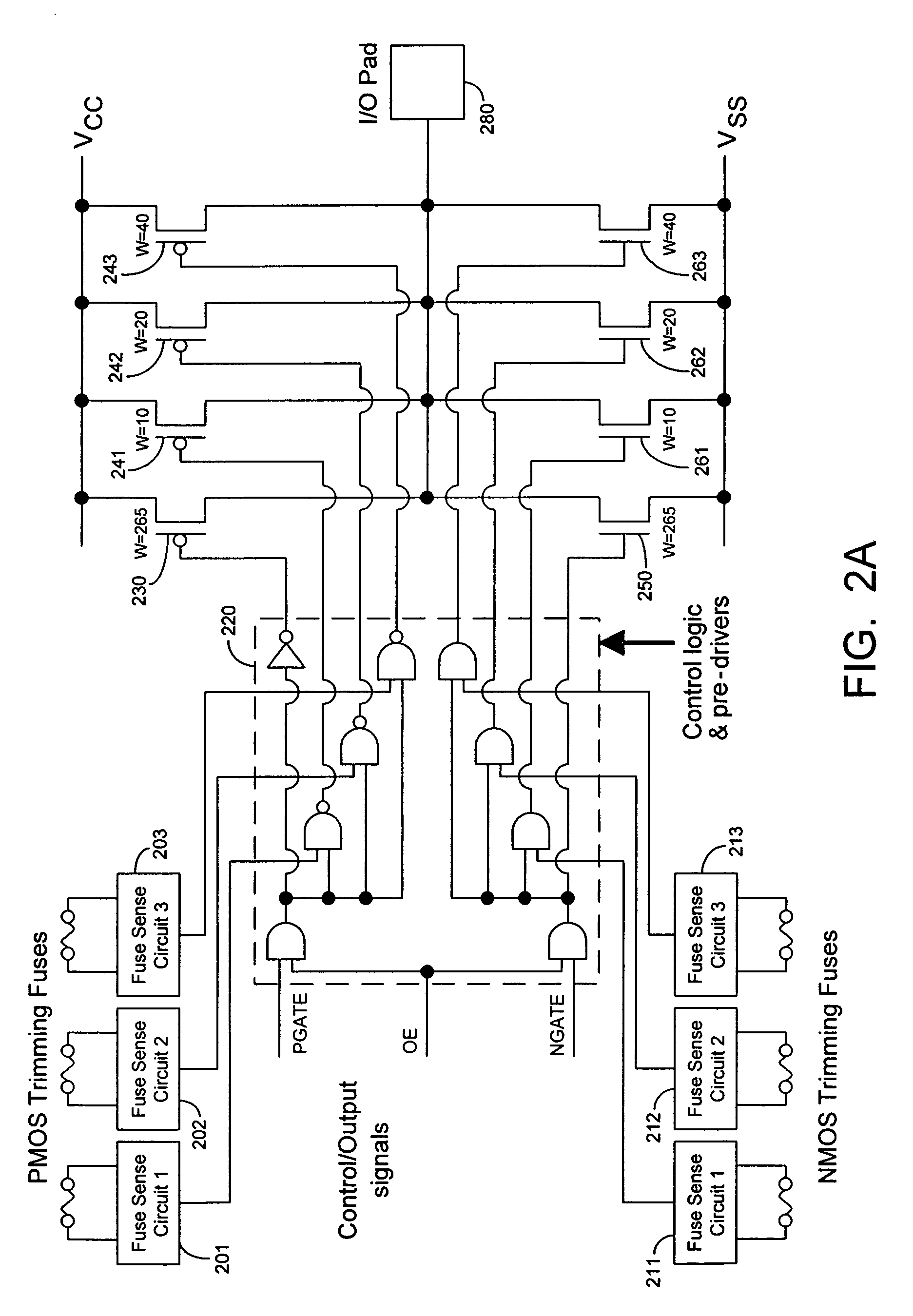
[0038]FIG. 2A illustrates an output driver with an adjustable drive current according to the present invention. The embodiment of FIG. 2A includes six fuse sense circuits 201, 202, 203, 211, 212, and 213. Each of the fuse sense circuits is coupled to a corresponding fuse. FIG. 2A also illustrates control logic and pre-driver block 220, main output drive transistors 230 and 250, output pad 280, and trimming transistors 241, 242, 243, 261, 262, and 263.

[0039]The drive and trimming transistor widths are shown in FIG. 2A in micrometers (μm). Transistor 230 has a width of 265 μm. The width of the pull up transistors can be increased by 10 μm by enabling transistor 241, 20 μm by enabling transistor 242, or 40 μm by enabling transistor 243. Alternatively, the width of the pull up transistors can be increased by 70 μm by enabling all three of transistors 241-243. Other combinations are possible for enabling one or more of trimming transistors 241-243. The width of the pull down transistors ...

third embodiment

[0043]FIG. 2B illustrates another output driver with an adjustable drive current according to the present invention. The output driver of FIG. 2B includes fuse sense circuits 301-305 and 311-315. Each of the fuse sense circuits is coupled to a corresponding fuse. FIG. 2B also illustrates control logic and pre-driver block 320, main output drive transistors 330 and 350, output pad 380, and trimming transistors 341-345 and 361-365. The drive and trimming transistor widths are shown in FIG. 2B in micrometers (μm). Any combination of one or more of the trimming transistors can be enabled to achieve a desired increase in the drive current.

[0044]When the fuse coupled to fuse sense circuit 301 is blown, block 320 enables pull-up trimming transistor 341 to be turned on or off by the pre-driver. If the fuse coupled to circuit 301 is not blown, block 320 disables trimming transistor 341. In a similar fashion, fuse sense circuits 302-305 and 311-315 control whether trimming transistors 342-345...


PUM


Abstract

Techniques are provided for trimming drive current in output drivers to compensate for process variations, model inaccuracies, and / or an off-target process. The actual output drive current is measured on the integrated circuit (IC) at wafer sort or during a final test. Based on the measured output drive current, the total transistor width that is required in the output driver to meet an I / O standard is calculated. A control block controls trimming transistors that are coupled in parallel with main output drive transistors. The control block adjusts the total width of the output drive transistors to bring the total width as close as possible to the desired width. Each I / O driver on a die can be adjusted individually based on its own drive current characteristics. All I / O drivers on a die can be adjusted by the same transistor width based on a single I / O measurement or on multiple I / O measurements.

Description

BACKGROUND OF THE INVENTION[0001]The present invention relates to techniques for trimming drive current in output drivers, and more particularly, to techniques for trimming drive current in output drivers to compensate for process variations and other abnormalities.[0002]Integrated circuits (ICs) typically contain output drivers that drive output signals from inside the chip to an external terminal for transmission off-chip. An output driver has at least one pull-up transistor and at least one pull-down transistor. These transistors are used to drive digital signals to an external terminal (also called a pad).[0003]The channel width-to-length (W / L) ratios (i.e., sizes) of the pull-up and pull-down transistors are typically chosen to meet a specific input / output (I / O) standard. Examples of I / O standards are LVTTL, LVCMOS, HSTL, GTL, and LVDS. Some integrated circuits support multiple version of an I / O standard for different supply voltages. For example, some ICs support 1.8 volt, 2.5...

Claims


Application Information

Patent Timeline
Patent Type & Authority Patents(United States)
IPC IPC(8): H03K19/094
CPCH03K17/145H03K17/164H03K19/00384
Inventor WATT, JEFFREY
Owner ALTERA CORP
Why Eureka
Try Eureka