Eureka AIR delivers breakthrough ideas for toughest innovation challenges, trusted by R&D personnel around the world.

Image sensor package and its manufacturing method

Active Publication Date: 2008-04-15
AMKOR TECH SINGAPORE HLDG PTE LTD
View PDF69 Cites 20 Cited by
  • Summary
  • Abstract
  • Description
  • Claims
  • Application Information

AI Technical Summary

Benefits of technology

[0010]Disclosed are an image sensor package and a method for manufacturing the same. A sealing portion is formed between an image sensor die and a glass substrate to completely isolate the sensing portion of the image sensor die from external environment. Electrically conductive bumps are formed outside of the sealing portion to electrically connect the image sensor die to the glass substrate. The image sensor die can be sealed by a cap while the image sensor die is connected to the glass substrate via the electrically conductive bumps. Even in this case, the sensing portion of the image sensor die is still completely isolated from external environment. Accordingly, no external alien substance or moisture can penetrate into the sensing portion of the image sensor die, and the image sensing capability is improved accordingly. The inter-coupling force between the image sensor die and the glass substrate is additionally improved.

Problems solved by technology

However, such conventional image sensor packages, which use an underfill having low viscosity, have a problem in that the underfill may flow to the sensing portion of the image sensor die and degrade the performance of the image sensor die.
This, of course, decreases the overall production yield of the package.
Such a large amount of moisture formed on the sensing portion, of course, degrades the sensing function of the image sensor package in a drastic manner.
This increases the overall size of the package.
Such an increase of size of the package acts as a hindrance to the current trend of making electronic products in a compact size.
This increases the manufacturing cost and makes the manufacturing process more complicated.
In particular, expensive underfill dispensing equipment increases the manufacturing cost of the package, and the additional underfill process, which must be performed after the glass substrate and the image sensor die are coupled to each other, makes the process more complicated.

Method used


Image

  • Image sensor package and its manufacturing method
  • Image sensor package and its manufacturing method
  • Image sensor package and its manufacturing method

Examples


Embodiment Construction

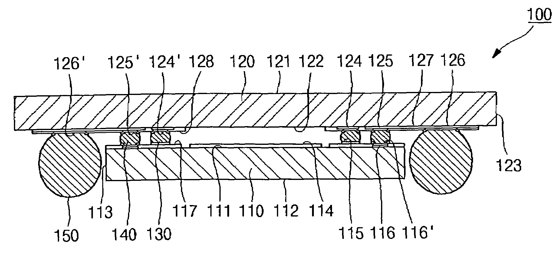
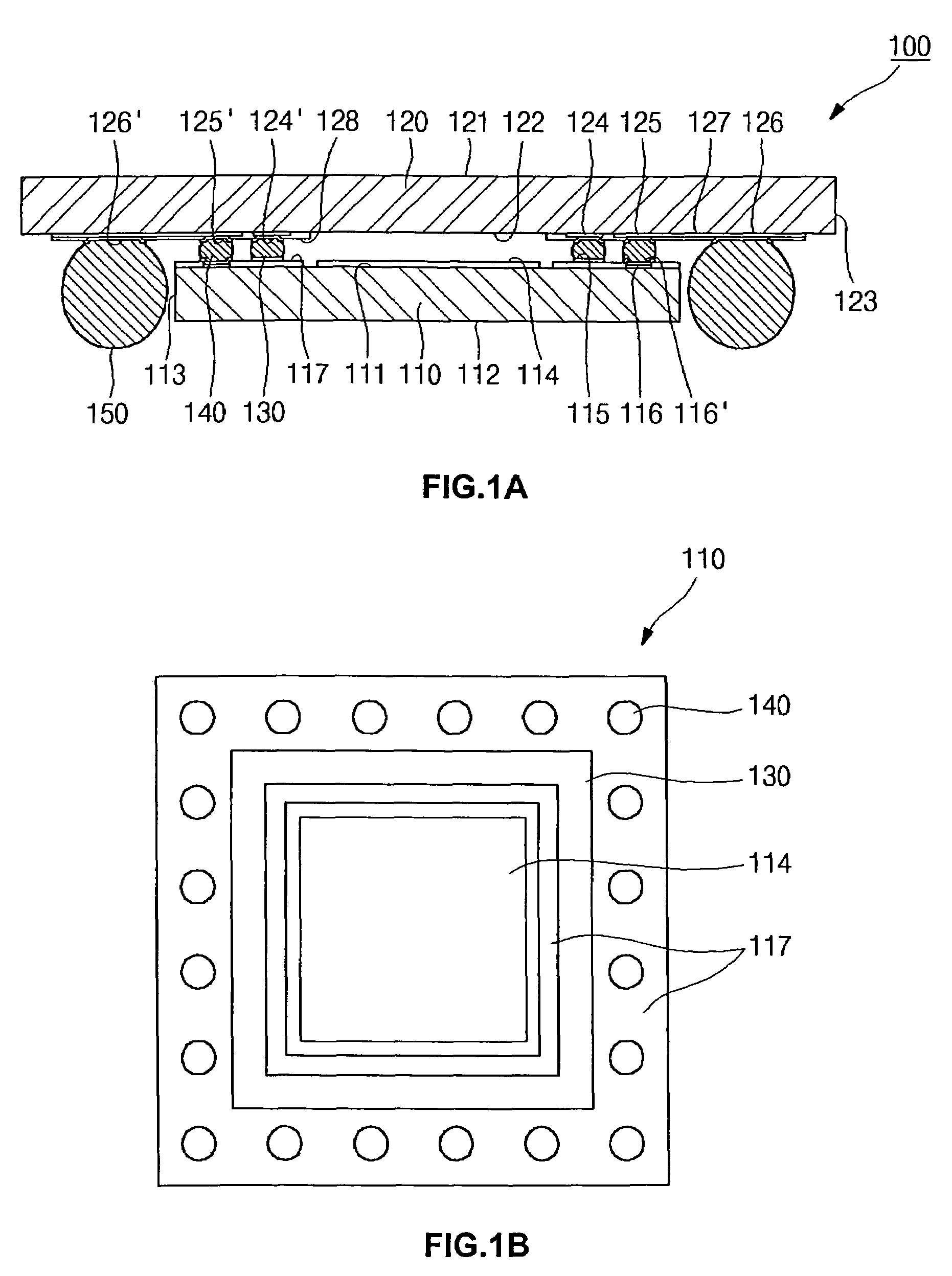
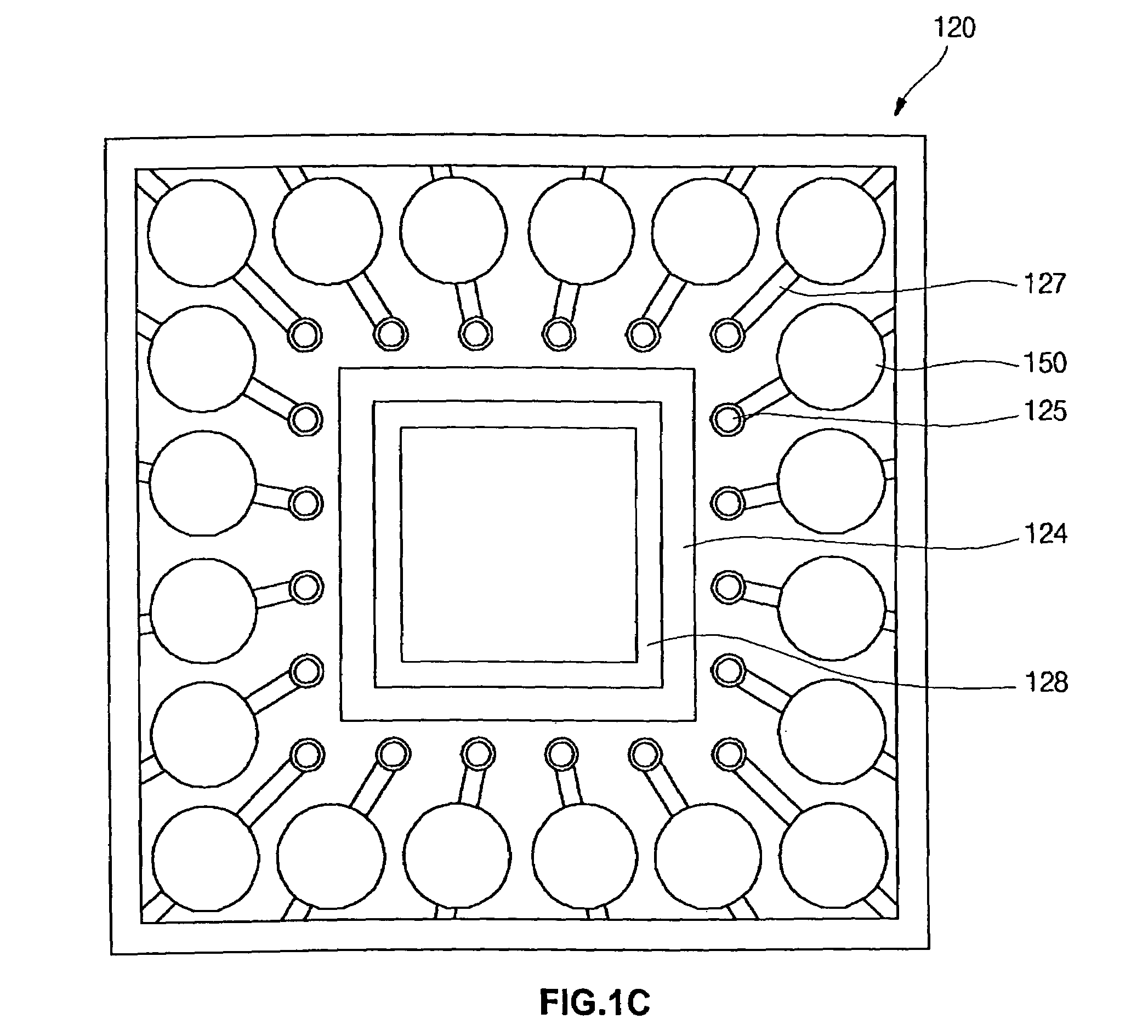
[0027]Referring to FIG. 1A, a sectional view of an image sensor package according to an embodiment of the present invention is shown, referring to FIG. 1B, a top view of an image sensor die is shown, and referring to FIG. 1C, a bottom view of a glass substrate is shown.

[0028]As shown, an image sensor package 100 according to the present invention includes an image sensor die 110 for sensing external images and converting them into electric signals, a glass substrate 120 for electrically connecting the image sensor die 110 to an external apparatus and stably retaining the image sensor die 110 on the external apparatus, a sealing portion 130 connected between the image sensor die 110 and the glass substrate 120 to prevent any external alien substance from penetrating into the sensing region of the image sensor die 110, a number of electrically conductive bumps 140 for electrically connecting the image sensor die 110 to the glass substrate 120, and a number of solder balls 150 for elec...


PUM


Abstract

Disclosed are an image sensor package and a method for manufacturing the same. A sealing portion is formed between an image sensor die and a glass substrate to completely isolate the sensing portion of the image sensor die from external environment. Electrically conductive bumps are formed outside of the sealing portion to electrically connect the image sensor die to the glass substrate. The image sensor die can be sealed by a cap while the image sensor die is connected to the glass substrate via the electrically conductive bumps.

Description

BACKGROUND OF THE INVENTION[0001]1. Field of the Invention[0002]The present invention relates to an image sensor package and its manufacturing method.[0003]2. Description of the Related Art[0004]In general, image sensors are devices which sense the information regarding objects to be photographed and transform it into video signals. Such devices may be classified into camera tubes, such as vidicons and plumbicons, and solid image sensors, such as complementary metal oxide semiconductors (CMOSs) and charge coupled devices (CCDs). When an image sensor is manufactured as the solid image sensor, it is generally used as a type of sensor wherein a lens is coupled to a semiconductor package which contains a semiconductor die for image sensors therein.[0005]Conventional image sensor packages are composed of a glass substrate having electrically conductive patterns formed thereon and an image sensor die coupled to the electrically conductive patterns of the glass substrate via electrically c...

Claims


Application Information

Patent Timeline
IPC IPC(8): G06K9/20
CPCH01L27/14618H01L27/14683H01L31/0203H01L2224/16H01L2224/05026H01L2224/05573H01L2224/05568H01L2224/05001H01L2224/05572H01L2224/05147H01L2224/05647H01L2924/00014
Inventor PAEK, JONG SIKJANG, HO CHEOLSEO, SEONG MIN
Owner AMKOR TECH SINGAPORE HLDG PTE LTD
Why Eureka
Eureka Blog
Learn More