Heater for heating a wafer and method for fabricating the same

a technology for heating and wafers, applied in the direction of ohmic resistance heating, heating arrangements of hot plates, lighting and heating apparatus, etc., can solve the problem of difficult to maintain the uniform heating balance of the wafer surface up to 0 and the in-plane temperature difference of the wafer, and achieve good production yield and mass production. , the effect of preventing resistance variation

Active Publication Date: 2008-04-22
KYOCERA CORP
View PDF8 Cites 154 Cited by
  • Summary
  • Abstract
  • Description
  • Claims
  • Application Information

AI Technical Summary

Benefits of technology

[0012]However, in the methods as described in the latter two Patent Documents, it is possible to improve the temperature distribution to a certain extent, but it is difficulty to lessen the in-plane temperature difference of the wafer up to 0.3° C. or lower.

Problems solved by technology

However, in the methods as described in the latter two Patent Documents, it is possible to improve the temperature distribution to a certain extent, but it is difficulty to lessen the in-plane temperature difference of the wafer up to 0.3° C. or lower.
Further, the heater formed in the above-mentioned method had a problem that the resistance value is varied during repetition of heating and cooling, and thereby a uniform heating balance of the wafer surface is not maintained to increase the temperature difference.

Method used


Image

  • Heater for heating a wafer and method for fabricating the same
  • Heater for heating a wafer and method for fabricating the same
  • Heater for heating a wafer and method for fabricating the same

Examples


example 1

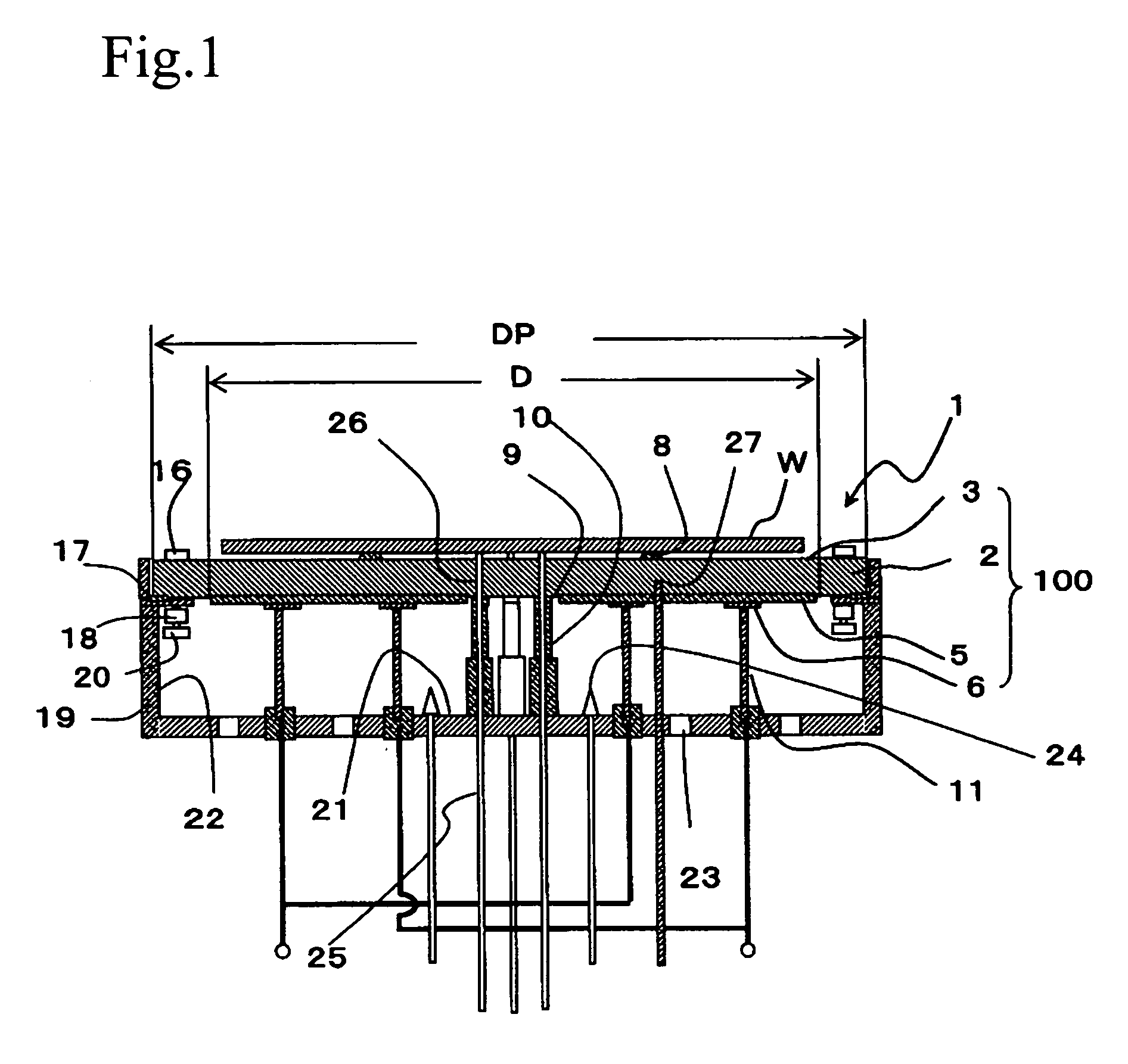
[0281]A silicon carbide sintered compact having thermal conductivity of 80 W / (m·K) was subjected to grinding to thus prepare a plurality of uniform heating plates taking a shape of a disc having a thickness of 4 mm and an outer diameter of 230 mm. In order to bond an insulating layer on one main surface of each uniform heating plate, a glass paste prepared by kneading ethyl cellulose as a binder and terpineol as an organic solvent with glass powder was laid by a screen printing method, heated at 150° C. to dry the organic solvent, defatted for 30 minutes at 550° C., and then subjected to baking at a temperature of 700 to 900° C. again. Thereby, the insulating layer composed of glass and having a thickness of 200 μm was formed. Subsequently, in order to bond a resistance heating element on the insulating layer, 20% by weight Au powder, 10% by weight Pt powder and 70% by weight glass as a conductive material were printed in a shape of a predetermined quantity of resistance heating ele...

example 2

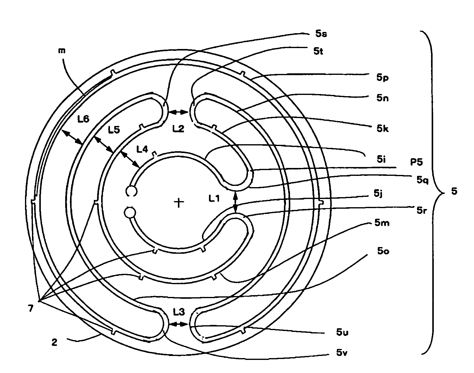
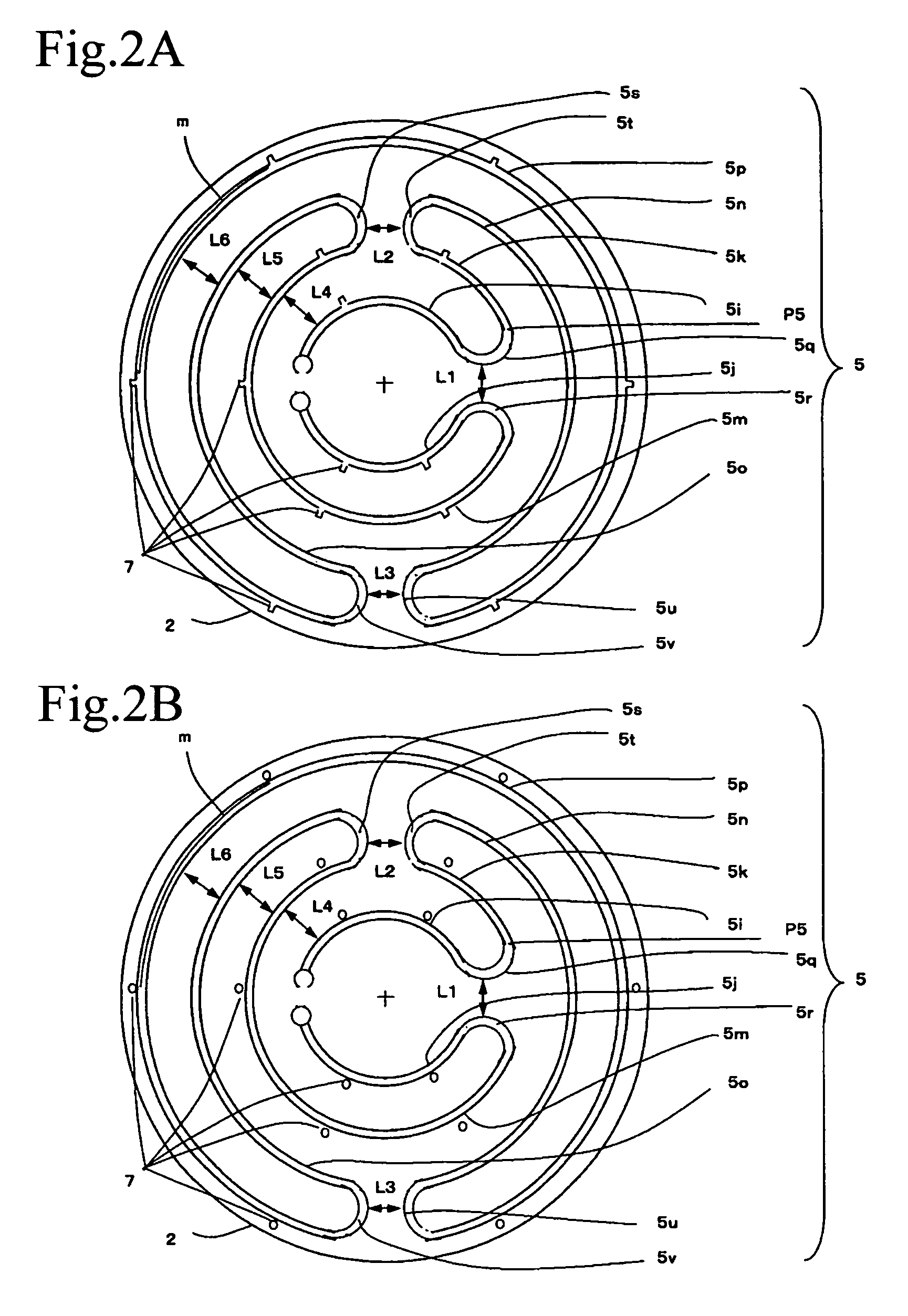
[0292]Samples were prepared in the same method as in Example 1. Further, the positioning mark configured of a protrusion shown in FIG. 6 was formed. Thereby, ceramic heaters forming a channel outside the belt, inside the belt, and in the middle of the belt were prepared. In addition, for the sake of comparison, a ceramic heater where the channels were present inside and outside was prepared.

[0293]Further, the belt of the resistance heating element was formed at a width of 1.5 mm, and then the belt was form with a group of channels by the laser. The channel group was formed on a portion of the belt located outside the plate shaped ceramics body. And, a sample changing an interval between the channel group and the channel group was prepared.

[0294]Further, the interval between the group and the group referred to dividing each resistance heating element zone of resistance heating elements into portions, lessening resistance deviation of each portion of each resistance heating element zo...

example 3

[0300]A silicon carbide sintered compact having thermal conductivity of 80 W / (m·K) was subjected to grinding to thus prepare a plurality of uniform heating plates taking a shape of a disc having a thickness of 4 mm and an outer diameter of 230 mm. In order to bond an insulating layer on one main surface of each uniform heating plate, a glass paste prepared by kneading ethyl cellulose as a binder and terpineol as an organic solvent with glass powder was laid by a screen printing method, heated at 150° C. to dry the organic solvent, defatted for 30 minutes at 550° C., and then subjected to baking at a temperature of 700 to 900° C. again. Thereby, the insulating layer composed of glass and having a thickness of 200 μm was formed. Subsequently, in order to bond a resistance heating element on the insulating layer, 20% by weight of Au powder, 10% by weight of Pt powder and 70% by weight of glass as a conductive material were printed in a shape of a predetermined quantity of pattern, and ...


PUM


Abstract

Provided is a heater capable of having a high uniform heating characteristic and substantially equally heating a wafer etc. mounted thereon, and a wafer heating device using the same, as well as a method thereof. The heater comprises a plate shaped body, a belt-like resistance heating element formed on the plate shaped body and having a channel for adjusting the resistance value, and a positioning mark formed on the plate shaped body, which serves as a reference for positioning the channel.

Description

BACKGROUND OF THE INVENTION[0001]1. Field of the Invention[0002]The present invention generally relates to a heater for heating a wafer, for example, a heater which is suitable for forming a thin film formed on a semiconductor wafer or a wafer of a liquid crystal display and a circuit board or the like, or for forming a resist film by drying and baking a resist solution applied on the wafer.[0003]2. Description of the Related Art[0004]In forming of a semiconductor thin film, etching, baking of a resist film, etc. in a process for fabricating a semiconductor, there is used a heater made of ceramics for heating a semiconductor wafer (hereinafter, abbreviated as a “wafer”).[0005]A conventional device for fabricating a semiconductor may be classified into a batch mode wherein a plurality of wafers are heated en bloc and a single mode wherein a plurality of wafers are heated one by one. In the single mode, since temperature controllability is excellent, a heater made of ceramics is widel...

Claims


Application Information

Patent Timeline
Patent Type & Authority Patents(United States)
IPC IPC(8): H05B3/68H05B3/16F23Q7/22H01L21/00H05B3/14
CPCH01L21/67103H05B3/143
Inventor MAKI, SEIICHIROUTAKENOUCHI, HIROSHIMASUYAMA, HIROYUKINAKAMURA, TSUNEHIKO
Owner KYOCERA CORP
Why Eureka
Try Eureka