
Stressed material and shape memory material MEMS devices and methods for manufacturing

a stress-based material and shape-based technology, applied in the field of stress-based material and shape-based shape-based material mems devices and manufacturing methods, can solve the problems of plastic deformation in the material, the size of the resulting mems devices is also unsatisfactory, and the un-deformed state is retained

Inactive Publication Date: 2008-05-13
PALO ALTO RES CENT INC
View PDF23 Cites 48 Cited by
  • Summary
  • Abstract
  • Description
  • Claims
  • Application Information

AI Technical Summary

Problems solved by technology

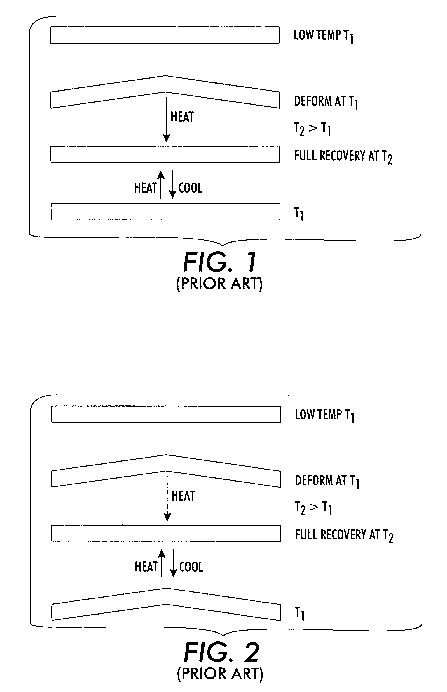
That is, once a SMA is recovered to its original, un-deformed state by heating to above the martensite-austenite phase transition temperature, it will retain the un-deformed state and can not be automatically returned to its previous deformed state upon cooling.
As the martensite phase has a low Young's modulus and a low yield strength, usually a small stress can induce a large deformation and cause plastic deformation in the material.
Additionally, the size of the resulting MEMS devices is also unsatisfactorily large.
At room temperature, the NiTi is in martensite phase and has a low Young's Modulus and low yield strength.
Similarly, many NiTi / Si bimorph devices are known which utilize the thermal mismatch between the NiTi film and a silicon substrate to generate residual stress, or different residual stresses when the NiTi is in martensite phase and austenite phase, which in turn result in displacement of the device.
Nonetheless, the application of such films in a MEMS actuator is so far limited and unsatisfactory, at least partially, because release of the metal film is also a “one-time-only” actuation.
That is, as previously explained with regard to SMA's, after being released and bent, it is very difficult to recover the metal film to its original flat state.
While it has been suggested to use electrostatic force to pull the film back to the original state, there are still many problems associated with that approach such as the very high applied voltage that would be needed.

Method used


Image

  • Stressed material and shape memory material MEMS devices and methods for manufacturing
  • Stressed material and shape memory material MEMS devices and methods for manufacturing
  • Stressed material and shape memory material MEMS devices and methods for manufacturing

Examples


example 1

Stressed Metal (MoCr) / SMA (TiNi) Film Actuator Model

[0091]An actuator was modeled having a length of 500 μm, a thickness of 3.75 μm, and a width of 100 μm. The actuator included a 1.75 μm-thick TiNi layer, a 1 μm thick MoCr layer with −1 GPa deposited compressive stress, and a 1 μm thick MoCr layer with +1 GPa deposited tensile stress. Tip displacement (μm) and spring constant (N / m) of the actuator are calculated and tabulated in Table 1, below.

example 2

Piezoelectric PZT Bimorph Actuator Model

[0092]An actuator also having a length of 500 μm, a thickness of 3.75 μm, and a width of 100 μm was modeled. The structure of the actuator included of two PZT films, each of which was 1.875 μm thick. Tip displacement (μm) and spring constant (N / m) of the actuator are calculated and tabulated in Table 1.

example 3

Si / Al Thermal Actuator Model

[0093]An actuator also having a length of 500 μm, a thickness of 3.75 μm, and a width of 100 μm was modeled. The structure of the actuator included a 1.5 μm thick Si film and 2.25 μm-thick Al film. Tip displacement (μm) and spring constant (N / m) of the actuator are calculated and tabulated in Table 1.


PUM

PropertyMeasurementUnit
phase transition temperatureaaaaaaaaaa
mechanical stressaaaaaaaaaa
compressive-tensile stressaaaaaaaaaa

Abstract

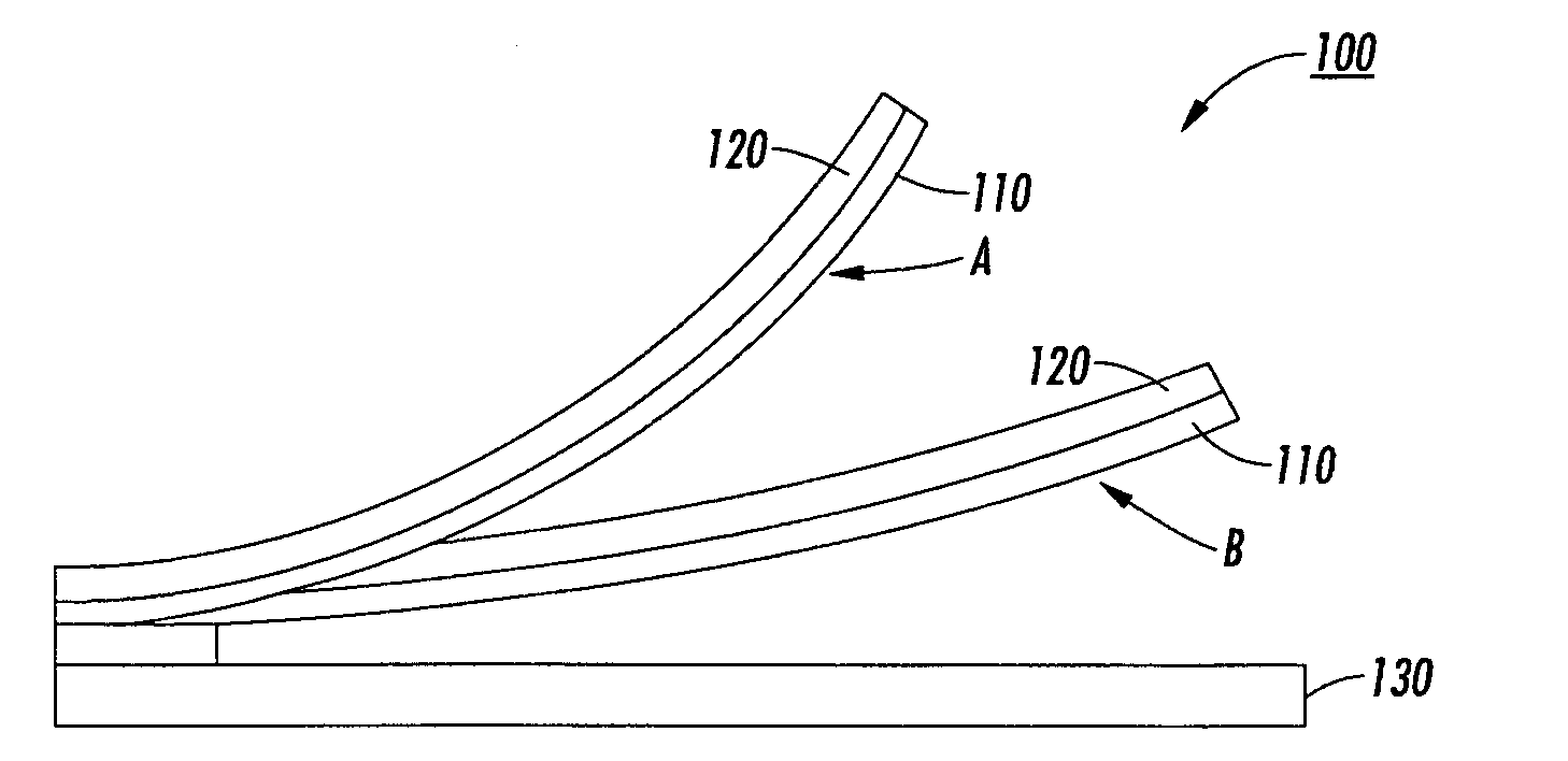
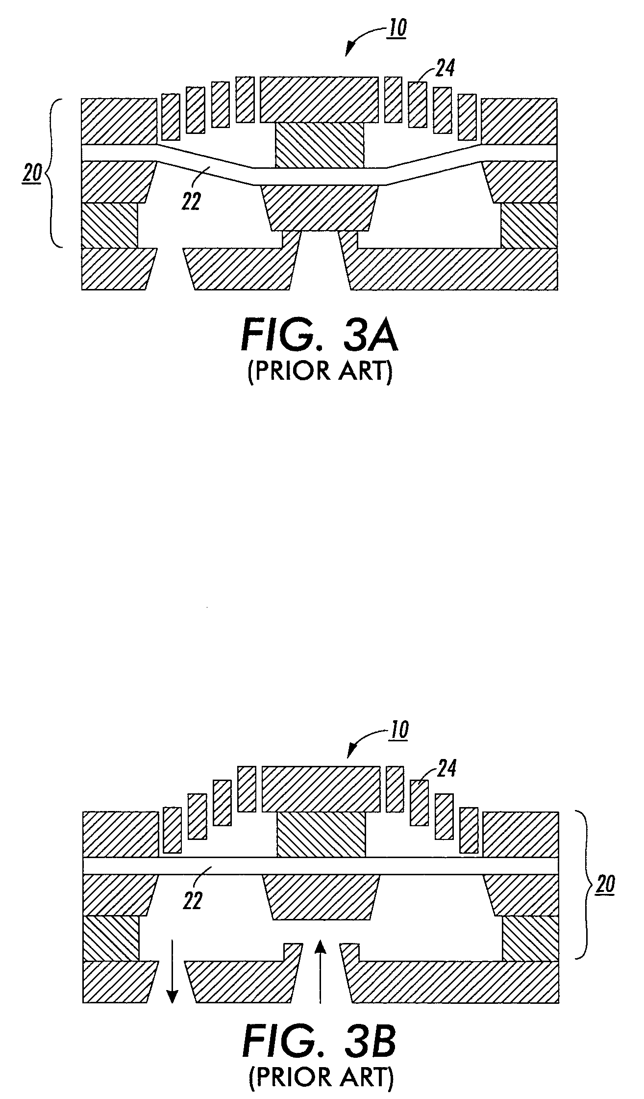
Disclosed is a MEMS device which comprises at least one shape memory material such as a shape memory alloy (SMA) layer and at least one stressed material layer. Examples of such MEMS devices include an actuator, a micropump, a microvalve, or a non-destructive fuse-type connection probe. The device exhibits a variety of improved properties, for example, large deformation ability and high energy density. Also provided is a method of easily fabricating the MEMS device in the form of a cantilever-type or diaphragm-type structure.

Description

BACKGROUND[0001]The present exemplary embodiment is generally related to MEMS devices and methods of manufacturing such devices. More particularly, the exemplary embodiment is related to a MEMS device comprising at least one shape memory material, such as a shape memory alloy layer and at least one stressed material layer. The device can be utilized as, for example, an actuator, a microswitch, a micropump, a microvalve, and a non-destructive fuse-type connection probe.[0002]Micro Electronic Mechanical Systems (MEMS) are microscopic devices and machines fabricated by integrating mechanical or hydraulic functions with electrical functions such as provided by computing / logic circuitry. MEMS technology has been widely utilized in a variety of industries. For example, a MEMS device can function as a sensing device, which combines a sensor and logic circuitry to perform monitoring functions such as pressure and acceleration measurement for deployment control of airbags in cars. A MEMS dev...

Claims


Application Information

Patent Timeline
Patent Type & Authority Patents(United States)
IPC IPC(8): H01H51/22
CPCF03G7/065F04B17/003G11C23/00H01L41/094F05C2201/0412F05C2203/0813F05C2251/00F05C2251/08H10N30/2042
Inventor XU, BAOMINFORK, DAVID KIRTLANDYOUNG, MICHAEL YU TAKCHOW, EUGENE MICHAEL
Owner PALO ALTO RES CENT INC
Learn More