Semiconductor integrated circuit device and manufacturing method thereof

Inactive Publication Date: 2005-04-07
RENESAS ELECTRONICS CORP
View PDF11 Cites 215 Cited by
  • Summary
  • Abstract
  • Description
  • Claims
  • Application Information

AI Technical Summary

Benefits of technology

[0035] When such metal boride is formed by irradiation with boron hydride gas, it is desirable to remove metal oxide from the surface of metal such as tungsten in advance. Such metal oxide can be removed by an aqueous ammonia solution. Doing so offers the advantage that only metal oxide on an exposed metal surface in the bottom of the opening (contact hole) can be removed, minimizing the possibility of accidental etching of silicon base interlayer insulating film formed on purpose or the silicon layer, without expansion of the contact hole in the metal wiring provided in the interlayer insulating film. In the process of making an opening by photolithography or dry etching, organic matter may remain in the bottom of the opening, which can interfere with the formation of metal boride as mentioned above. This organic matter can be removed by irradiation with ultraviolet light. However, some

Problems solved by technology

In the process of making an opening by photolithography or dry etching, organic matter may remain in the bottom of the opening, which can interfere with the formation of metal boride as mentioned above.
However, some kind of organic matter m

Method used


Image

  • Semiconductor integrated circuit device and manufacturing method thereof
  • Semiconductor integrated circuit device and manufacturing method thereof
  • Semiconductor integrated circuit device and manufacturing method thereof

Examples


first embodiment

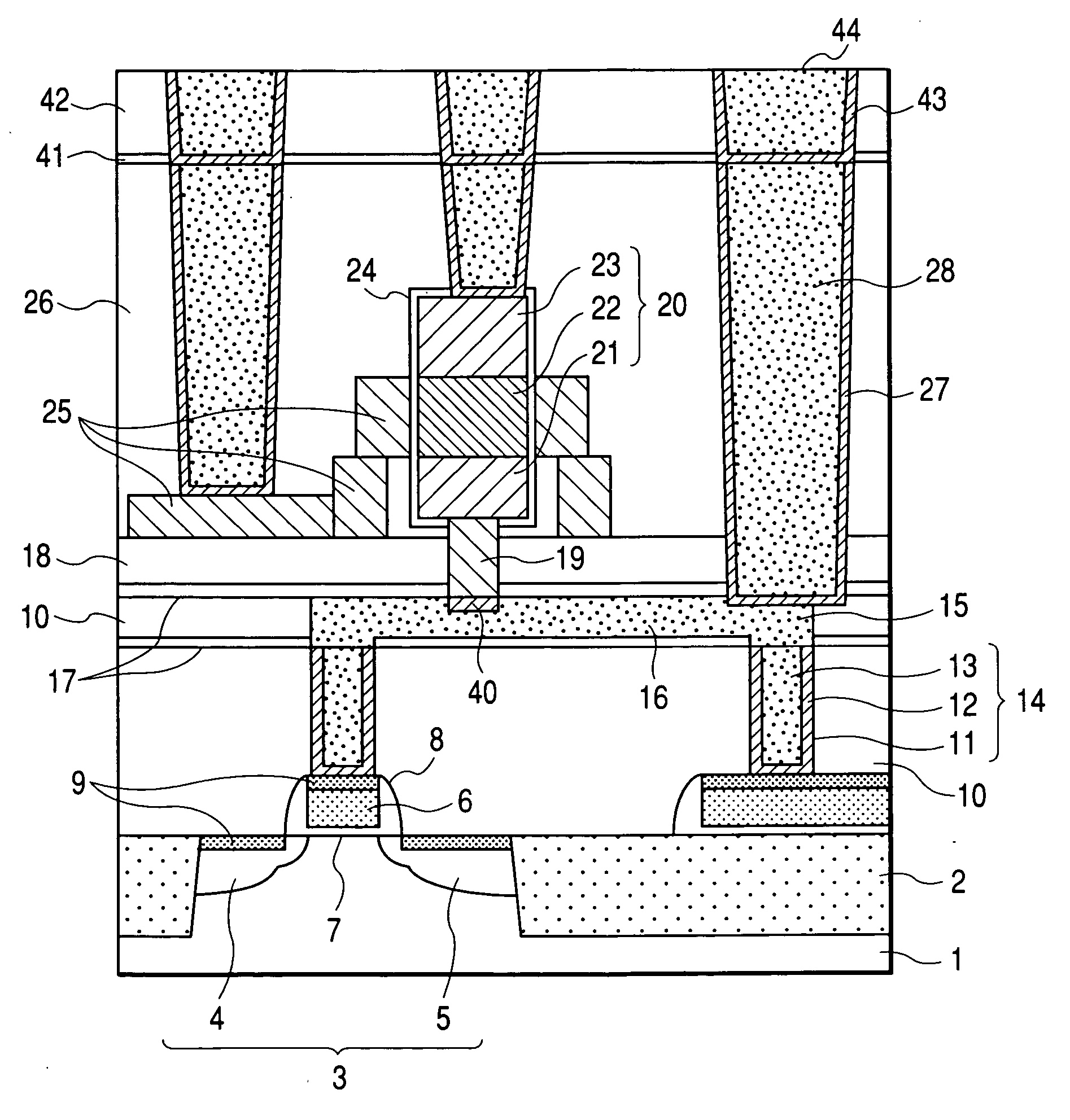
[0064] For illustration of this embodiment, the process of experimentation which was conducted in order to solve the problems to be solved by the present invention, and phenomena observed in the process will be described next. High temperature heat treatment for oxidization to form gate oxide film is necessary to make a vertical MOS transistor 20 or a horizontal MOS transistor 29 over the silicon plug 19. It was predicted that this high temperature heat treatment process might cause silicide reaction between the tungsten wiring 16 and the silicon plug 19, leading to film peeling or tungsten diffusion up to the upper MOS transistor with a resultant deterioration in transistor characteristics. For this reason, we explored a method of suppressing this sort of reaction in the interfaces. For the purpose of reaction suppression, on the analogy of the known polymetal gate and polycide gate structure mentioned earlier, we inserted a barrier layer between the tungsten wiring 16 and the sili...

second embodiment

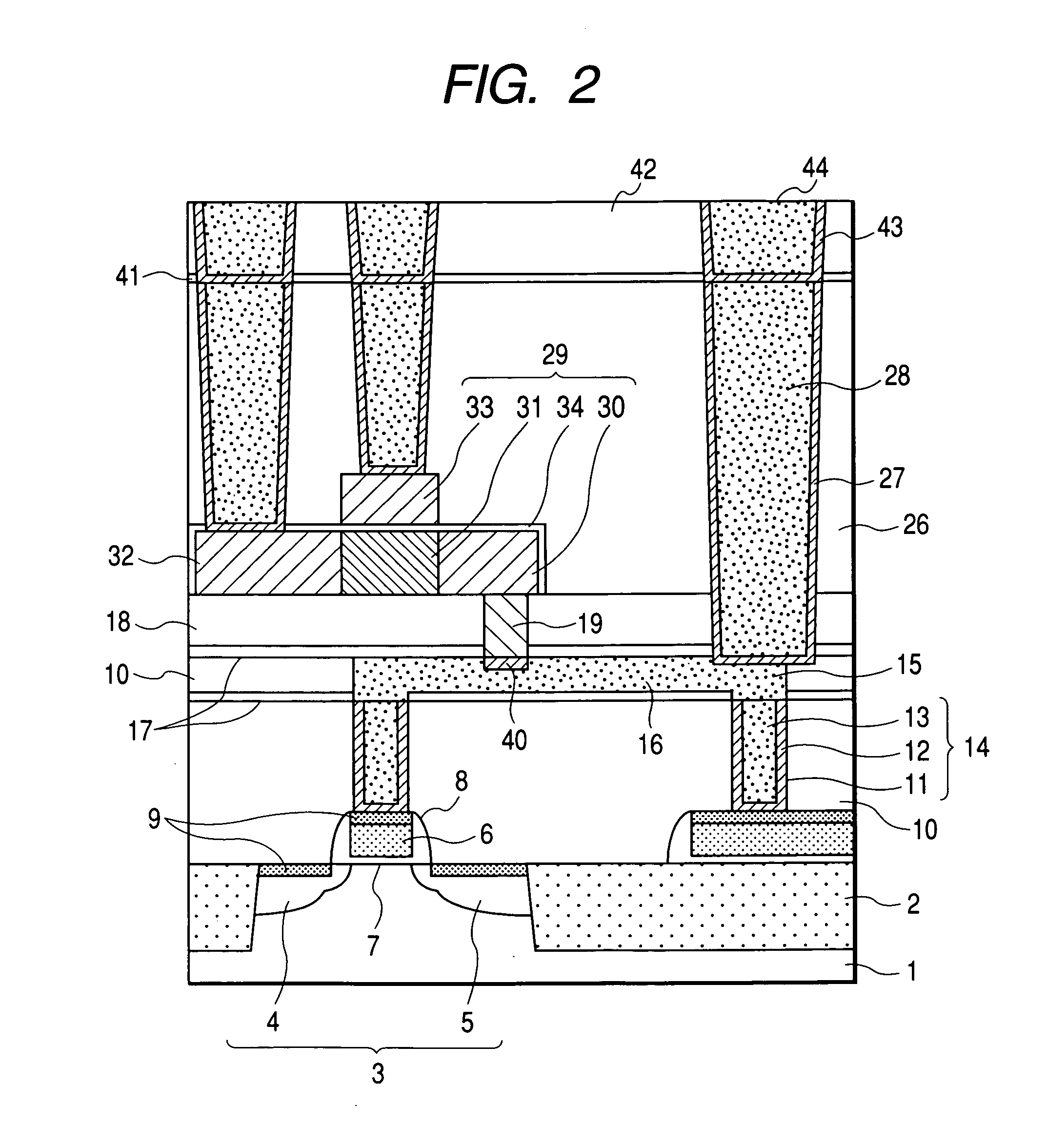
[0070] According to the first embodiment, the metal boride 40 is formed by irradiating the tungsten film surface with boron hydride gas 37. According to this embodiment, for the above semiconductor integrated circuit devices shown in FIG. 1 and FIG. 2, an opening for the silicon plug 19 is made at a given position on the tungsten wiring 16 and then boron ions are implanted into the tungsten film surface in the bottom of the opening at 5×10¹⁴ atoms / cm2 (5 keV). If boron ions should be directly implanted into the tungsten wiring 16, channeling of implanted ions would occur in the film and it would be difficult to form metal boride 40 on the tungsten wiring 16 surface. For this reason, in this embodiment, in the process of making an opening in the tungsten wiring 16 (FIGS. 1 and 2), only the interlayer insulating film 18 is removed by dry etching while the 30 nm thick silicon nitride film 17 formed by plasma CVD remains intact. Then, boron ions are implanted through this non-crystallin...

third embodiment

[0077] If a relatively thick layer of natural tungsten oxide exists on the tungsten film 19, it will be difficult to form the boride 40 as seen in the first embodiment. In this embodiment, although reaction does not occur between the tungsten wiring 16 and the silicon plug 19 in high temperature heat treatment as in the second embodiment, metal oxide reduction reaction occurs due to the silicon and consequently a silicon oxide layer is formed in the interface. In some cases, the contact resistance between the metal and silicon is 10−5 ohm-cm2 or more, or the semiconductor device delivers particular electric conductivity characteristics attributable to the presence of insulator in the interface.

[0078] Therefore, for formation of metal boride, it is necessary to remove metal oxide such as tungsten oxide as much as possible. Hence, this embodiment is intended to provide a method of removing such metal oxide and a process of fabricating a semiconductor integrated circuit device in acco...


PUM


Abstract

A manufacturing process for a semiconductor integrated circuit device which prevents occurrence of reaction between metal wiring and a boron-doped silicon plug over it in heat treatment for a MOS transistor to be formed over them and reduces the possibility of rise in contact resistance. Metal boride is formed on an exposed metal surface in the bottom of an opening made in an interlayer insulating film over the metal wiring. In order to facilitate formation of such metal boride, metal oxide remaining on the metal surface is removed with an aqueous ammonia solution. The meal surface is irradiated with high energy ultraviolet light in order to remove organic matter remaining in the opening and facilitate removal of the metal oxide with the aqueous ammonia solution.

Description

FIELD OF THE INVENTION [0001] The present invention relates to a semiconductor integrated circuit device and manufacturing technology thereof and more particularly to a semiconductor integrated circuit device which has a polycrystalline silicon layer over a metal layer and technology which is effective for the manufacture thereof. BACKGROUND OF THE INVENTION [0002] In a semiconductor integrated circuit device structure in which a layer of metal such as tungsten is laid over a silicon substrate or polycrystalline silicon, it is common to provide a reaction suppression layer (barrier layer) in the interface between the metal layer and the silicon layer, as exemplified by the techniques disclosed in patent documents 1 to 4 (listed below). Also, techniques which concern a polymetal gate as a kind of multi-layer gate electrode are described in patent documents 5 to 21 and non-patent documents 1 to 3. [0003] For a polycide gate which has tungsten silicide (tungsten silicon compound) over ...

Claims


Application Information

Patent Timeline
IPC IPC(8): H01L21/02H01L21/768H01L21/28H01L21/336H01L21/822H01L21/8238H01L21/8242H01L27/00H01L27/06H01L27/08H01L27/092H01L29/78H01L29/786
CPCH01L21/02063H01L21/76843H01L21/76849H01L21/76867H01L21/76886H01L2924/0002H01L21/8221H01L27/0688H01L2924/00H01L21/0455H01L21/26533H01L21/28229H01L21/76805
Inventor YAMAMOTO, NAOKINISHIDA, AKIOFUJIMOTO, AKIRACHAKIHARA, HIRAKUMATSUOKA, HIDEYUKIMINE, TOSHIYUKI
Owner RENESAS ELECTRONICS CORP
Why Eureka
Try Eureka