Liquid crystal display device

a liquid crystal display and display device technology, applied in static indicating devices, non-linear optics, instruments, etc., can solve the problems of difficult to realize stable production of devices, narrow viewing angle of conventional twist nematic and super twist nematic liquid crystal display devices, and high probability of rubbing streaks in displayed images. achieve the effect of wide viewing angle, high continuity, and improved display quality of conventional liquid crystal display devices

Active Publication Date: 2008-05-20
SHARP KK
View PDF120 Cites 38 Cited by
  • Summary
  • Abstract
  • Description
  • Claims
  • Application Information

AI Technical Summary

Benefits of technology

[0010]It is therefore an object of this invention to provide a transmission-reflection liquid crystal display device having a wide viewing angle characteristic, a high display quality, and a high aperture ratio, and being capable of producing a bright display.
[0039]According to the present invention, a liquid crystal domain having a radially-inclined orientation is stably formed with a high degree of continuity. Therefore, it is possible to further improve the display quality of a conventional liquid crystal display device having a wide viewing angle characteristic.
[0040]Moreover, a multigap structure is realized by providing a stepped portion on a substrate different from the substrate that is provided with an electrode for producing an inclined electric field for forming a radially-inclined orientation, whereby it is possible to obtain advantages related to the production process. Since the side surface of the stepped portion is located in the reflection region while being covered with the electrode, it is possible to suppress the deterioration in the display quality due to the inclination of the side surface of the stepped portion.
[0041]Furthermore, in each picture element region, a plurality of sub-electrodes are arranged in a line in a predetermined direction, whereby it is possible to increase the area ratio of the sub-electrode in the picture element region, thus improving the aperture ratio.
[0042]Picture elements that are adjacent to each other in a direction crossing the sub-electrode arrangement direction are driven with voltages of opposite polarities in each frame, whereby it is possible to produce an inclined electric field having a sharp potential gradient between picture elements that are adjacent to each other in that direction. Thus, it is possible to form a sufficiently stable radially-inclined orientation even when employing an arrangement with a short inter-electrode distance and a high aperture ratio.
[0043]As described above, the present invention provides a transmission-reflection liquid crystal display device having a wide viewing angle characteristic, a high display quality, and a high aperture ratio, and being capable of producing a bright display.

Problems solved by technology

However, conventional twist nematic (TN) type and super twist nematic (STN) type liquid crystal display devices have a narrow viewing angle.
While the transverse electric field mode is an effective approach to improve the viewing angle, the production process thereof imposes a significantly lower production margin than that of a normal TN type device, whereby it is difficult to realize stable production of the device.
However, when a vertical alignment film is subjected to a rubbing treatment, rubbing streaks are likely to appear in the displayed image, and it is not suitable for mass-production.
Moreover, optimal configurations have not yet been found for cases where the alignment control using an inclined electric field is applied to a transmission-reflection liquid crystal display device.

Method used


Image

  • Liquid crystal display device
  • Liquid crystal display device
  • Liquid crystal display device

Examples


embodiment 1

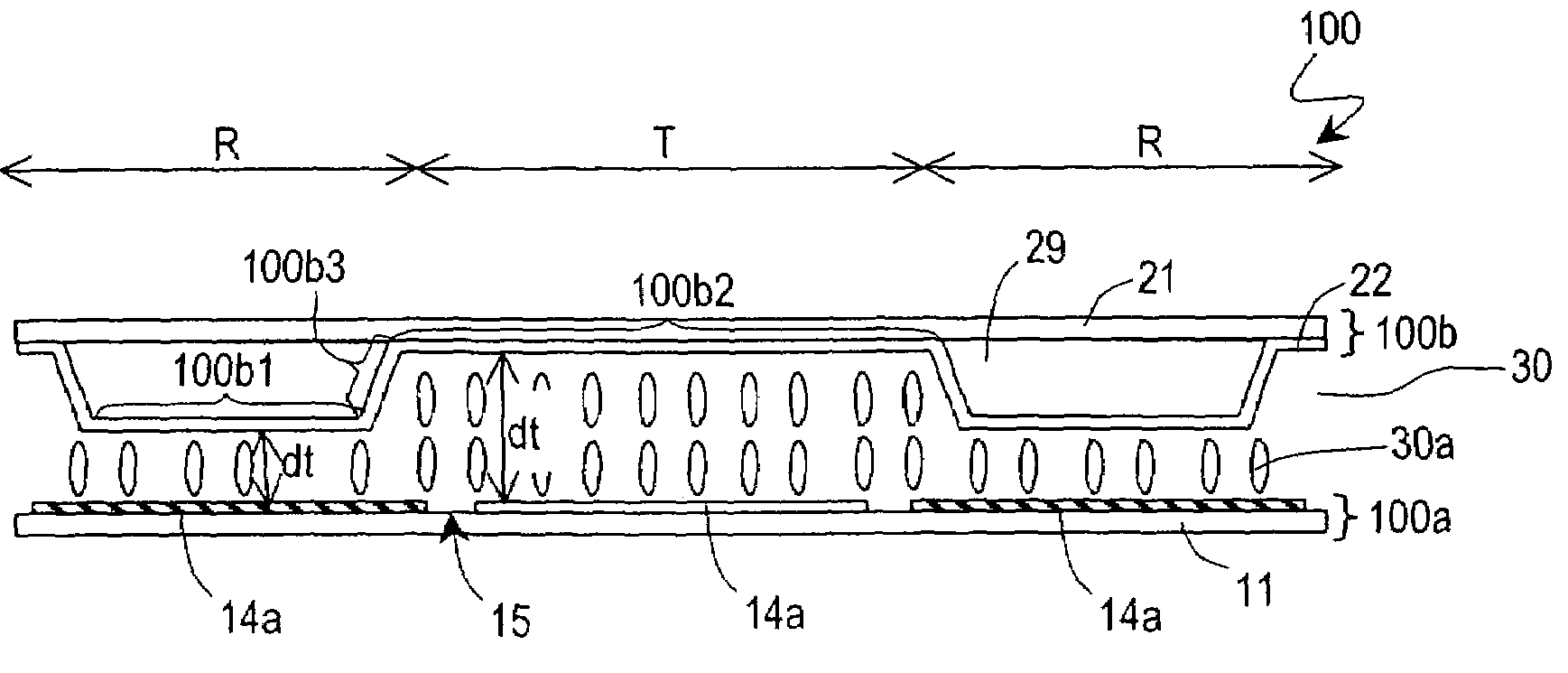
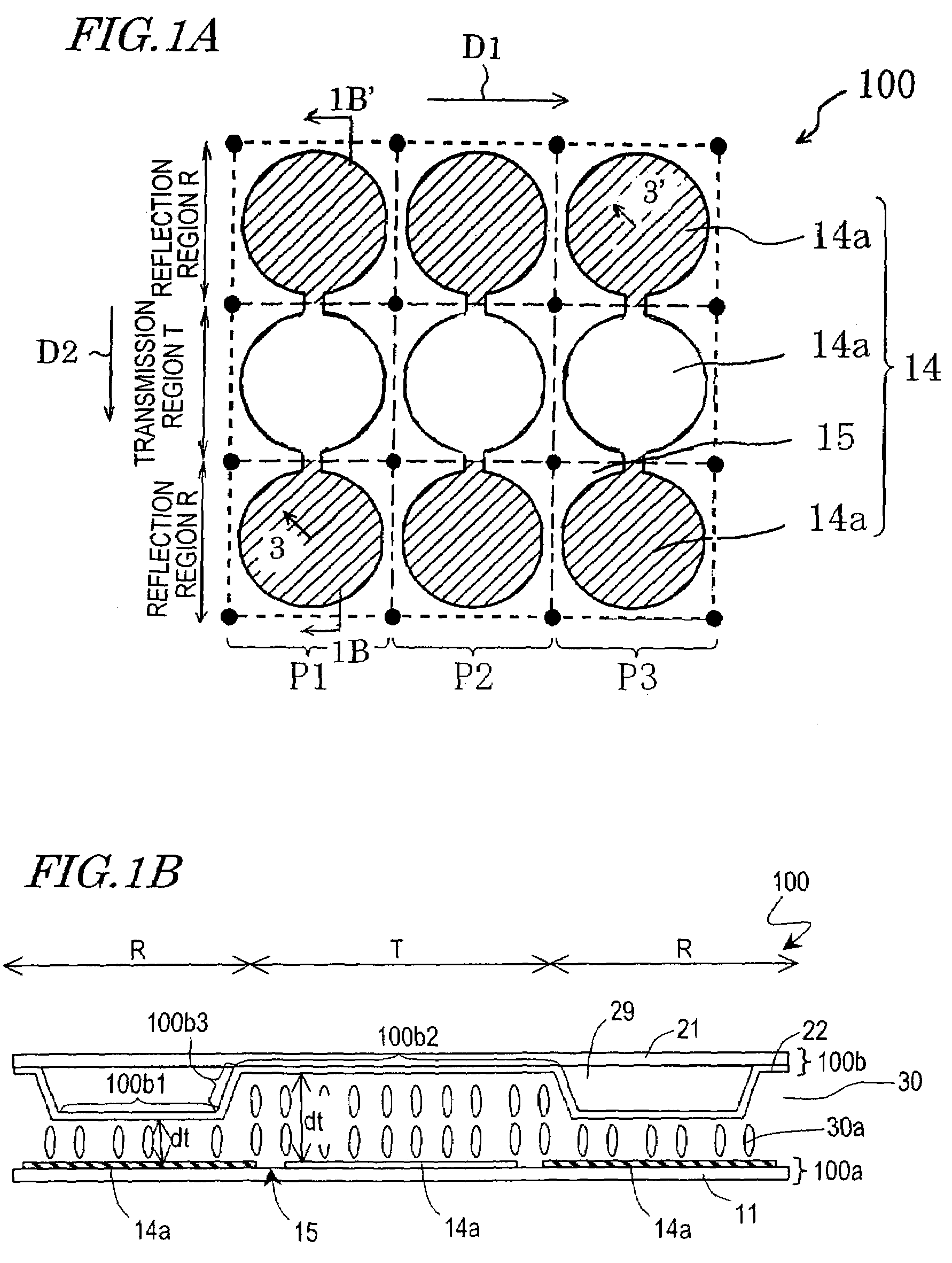
[0084]The structure of a liquid crystal display device 100 according to the present embodiment will now be described with reference to FIG. 1A and FIG. 1B. In the following description, a color filter and a black matrix are omitted for the sake of simplicity. Moreover, in subsequent figures, each element having substantially the same function as the corresponding element in the liquid crystal display device 100 will be denoted by the same reference numeral and will not be further described below. FIG. 1A is a plan view illustrating three picture element regions P1, P2 and P3 of the liquid crystal display device 100 as viewed in the substrate normal direction, and FIG. 1B is a cross-sectional view taken along line 1B-1B′ of FIG. 1A. FIG. 1B illustrates a state where no voltage is applied across a liquid crystal layer.

[0085]The liquid crystal display device 100 includes an active matrix substrate (hereinafter referred to as a “TFT substrate”) 100a, a counter substrate (referred to als...

embodiment 2

[0168]The liquid crystal display device of the present embodiment is different from the liquid crystal display device 100 of Embodiment 1 in that the counter substrate includes an orientation-regulating structure.

[0169]FIG. 19A to FIG. 19E schematically illustrate a counter substrate 200b having an orientation-regulating structure 28. Each element having substantially the same function as that of the liquid crystal display device 100 will be denoted by the same reference numeral and will not be further described.

[0170]The orientation-regulating structure 28 illustrated in FIG. 19A to FIG. 19E functions to orient the liquid crystal molecules 30a of the liquid crystal layer 30 into a radially-inclined orientation. Note that the orientation-regulating structure 28 illustrated in FIG. 19A to FIG. 19D and that illustrated in FIG. 19E are different in terms of the direction in which the liquid crystal molecules 30a are to be inclined.

[0171]The direction in which the liquid crystal molecul...

embodiment 3

[0216]A liquid crystal display device 300 of the present embodiment will now be described with reference to FIG. 36. The liquid crystal display device 300 is different from the liquid crystal display device 100 illustrated in FIG. 1A and FIG. 1B in that the thickness de of the liquid crystal layer 30 at an edge portion of the sub-electrode 14a placed in the transmission region T is smaller than the thickness dc of the liquid crystal layer 30 at a central portion of the sub-electrode 14a, as illustrated in FIG. 36.

[0217]The response speed of the liquid crystal molecules 30a is typically higher as the thickness of the liquid crystal layer 30 (cell gap) is smaller (whereby the effect of the electric field is more significant), and it is generally inversely proportional to the square of the thickness of the liquid crystal layer 30. Therefore, if the thickness de of the liquid crystal layer 30 at the edge portion (outer periphery) of the sub-electrode 14a is smaller than the thickness dc...


PUM

PropertyMeasurementUnit
angleaaaaaaaaaa
widthaaaaaaaaaa
widthaaaaaaaaaa

Abstract

In each picture element region, a first electrode provided on one side of the first substrate that is closer to the liquid crystal layer includes a plurality of sub-electrodes, whereby the liquid crystal layer forms a liquid crystal domain taking a radially-inclined orientation above each sub-electrode by an inclined electric field produced around the sub-electrode. The second substrate includes a stepped portion including an upper tier located in the reflection region, a lower tier located in the transmission region and a side surface connecting the upper tier and the lower tier to each other, the side surface of the stepped portion being located in the reflection region and covered by the second electrode. The plurality of sub-electrodes are arranged in a line in a column direction D2, and picture elements that are adjacent to each other in a row direction D1 are driven with voltages of opposite polarities in each frame.

Description

FIELD OF THE INVENTION[0001]The present invention relates to a liquid crystal display device, and more particularly to a liquid crystal display device having a wide viewing angle characteristic and being capable of producing a high quality display.BACKGROUND OF THE INVENTION[0002]In recent years, liquid crystal display devices, which are thin and light in weight, are used as personal computer displays and PDA (personal digital assistance) displays. However, conventional twist nematic (TN) type and super twist nematic (STN) type liquid crystal display devices have a narrow viewing angle. Various technical developments have been undertaken to solve the problem.[0003]A typical technique for improving the viewing angle characteristic of a TN or STN type liquid crystal display device is to add an optical compensation plate thereto. Another approach is to employ a transverse electric field mode in which a horizontal electric field with respect to the substrate plane is applied across the ...

Claims


Application Information

Patent Timeline
Patent Type & Authority Patents(United States)
IPC IPC(8): G02F1/1335G02F1/1337G02F1/1333G02F1/133G02F1/1343G02F1/136G02F1/139
CPCG02F1/133555G02F1/1393G02F1/134309G02F1/1337
Inventor KUBO, MASUMI
Owner SHARP KK
Why Eureka
Try Eureka