Gas valve assembly and apparatus using the same

a gas valve and assembly technology, applied in the direction of coatings, chemical vapor deposition coatings, metallic material coating processes, etc., can solve the problem of large installation area, and achieve the effect of preventing the contamination of the chamber due to preventing the leakage of magnetic fluid

Active Publication Date: 2008-06-03
JUSUNG ENG
View PDF30 Cites 15 Cited by
  • Summary
  • Abstract
  • Description
  • Claims
  • Application Information

AI Technical Summary

Benefits of technology

[0010]Another object of the present invention is to provide a gas valve assembly where a leakage of a magnetic fluid is prevented.
[0011]Another object of the present invention is to provide an atomic layer deposition apparatus using a gas assembly where a contamination of chamber due to a leakage of a magnetic fluid is prevented.

Problems solved by technology

However, since an ALD apparatus includes a plurality of injecting pipes and a plurality of valves adjusting the plurality of injecting pipes, a large installation area is required.

Method used


Image

  • Gas valve assembly and apparatus using the same
  • Gas valve assembly and apparatus using the same
  • Gas valve assembly and apparatus using the same

Examples


Embodiment Construction

[0024]Reference will now be made in detail to the preferred embodiments, examples of which are illustrated in the accompanying drawings.

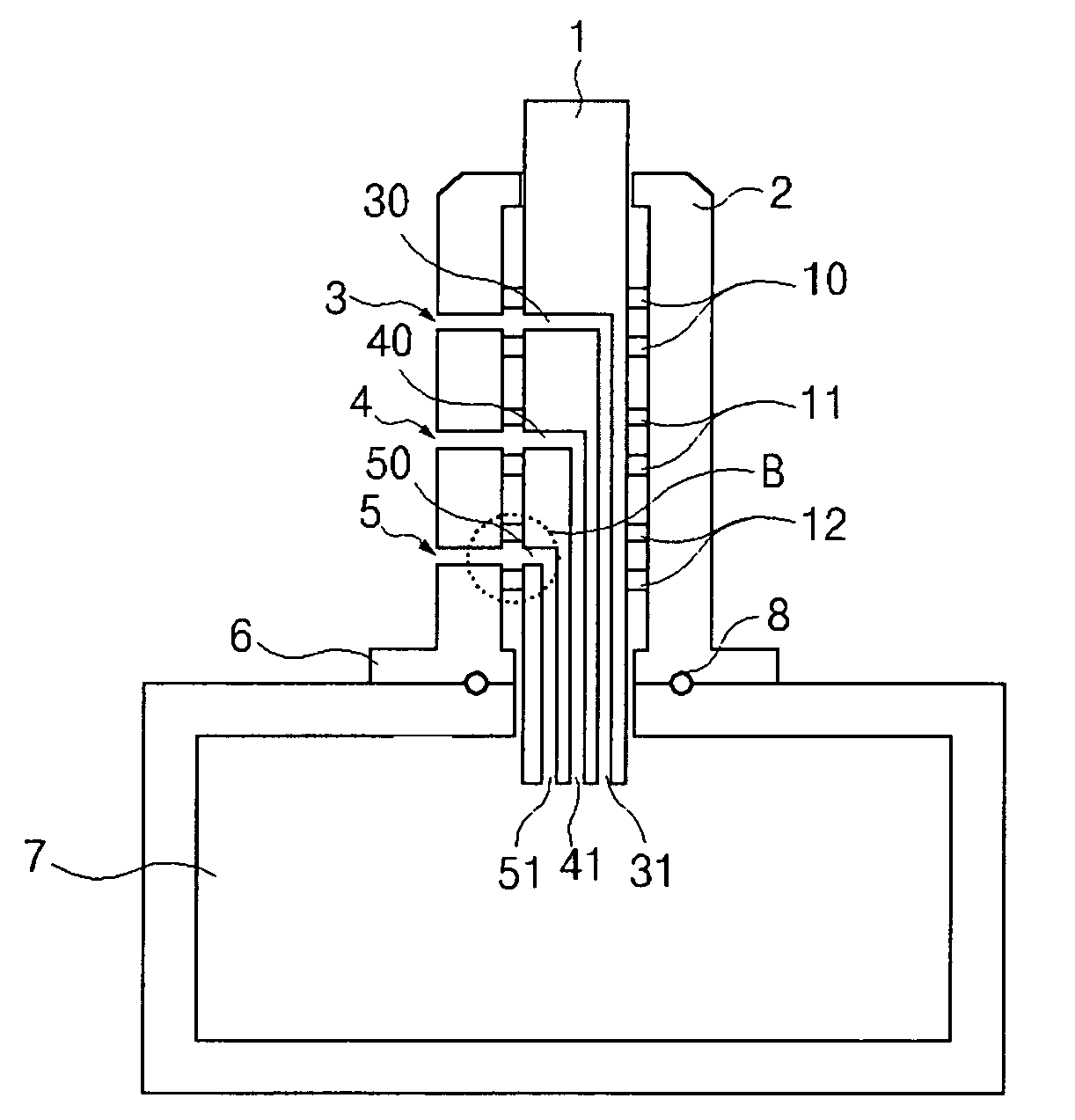
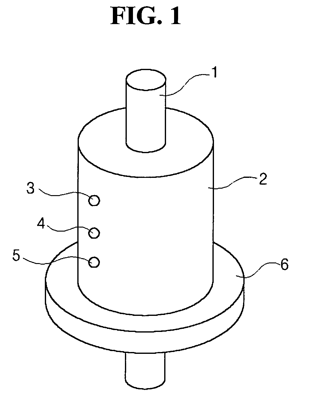
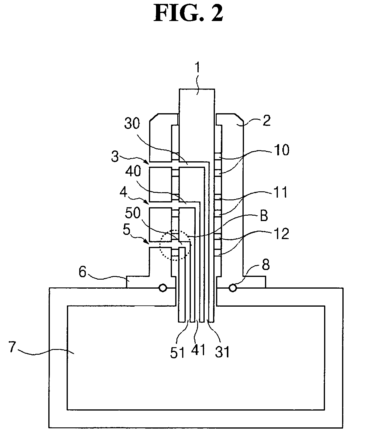
[0025]FIG. 1 is a schematic perspective view of a gas assembly for an atomic layer deposition apparatus according to an embodiment of the present invention, and FIG. 2 is a schematic cross-sectional view of an atomic layer deposition apparatus having a gas assembly according to an embodiment of the present invention.

[0026]In FIGS. 1 and 2, a gas assembly includes a driving shaft 1, a housing 2 surrounding the driving shaft 1 and a flange 6. The driving shaft 1 rotates using a power supplied from a driving unit (not shown) and first, second and third gas supply paths 30, 40 and 50 may be formed in the driving shaft 1. In addition, first, second and third through holes 3, 4 and 5 may be formed in a sidewall of the housing 2. The flange 6 may be combined to a chamber 7 of the atomic layer deposition (ALD) apparatus using a combination means such as a b...


PUM

PropertyMeasurementUnit
sizeaaaaaaaaaa
shapeaaaaaaaaaa
cylindrical shapeaaaaaaaaaa

Abstract

A gas valve assembly for a deposition apparatus includes: a driving shaft including a plurality of gas supply paths therein; a housing surrounding the driving shaft and including a plurality of through holes therein; a plurality of magnetic seal pairs between the driving shaft and the housing, the plurality of magnetic seal pairs including a magnetic fluid; and a leakage-preventing means between the driving shaft and the housing, the leakage-preventing means preventing a leakage of the magnetic fluid.

Description

[0001]The present invention claims the benefit of Korean Patent Application No. 2003-39028 filed in Korea on Jun. 17, 2003, which is hereby incorporated by reference.BACKGROUND OF THE INVENTIONField of the Invention[0002]The present invention relates to a gas valve assembly for an atomic layer deposition apparatus, and more particularly, to a gas valve assembly having a magnetic seal.DISCUSSION OF THE RELATED ART[0003]In general, a semiconductor device or a liquid crystal display (LCD) device is formed through a fabricating process for a substrate including a deposition step of a thin film, an etching step and a cleaning step. As the substrate, a wafer may be used for a semiconductor device while a glass substrate may be used for an LCD device.[0004]Methods of forming a thin film may be classified into a physical vapor deposition (PVD) method using a physical impact and a chemical vapor deposition (CVD) method using a chemical reaction. Since a thin film by a CVD method has superior...

Claims


Application Information

Patent Timeline
Patent Type & Authority Patents(United States)
IPC IPC(8): C23C16/455C23F1/00H01L21/306C23C16/44H01L21/20
CPCC23C16/4401C23C16/45574C23C16/45544C23C16/4409H01L21/20
Inventor LEE, SANG-GON
Owner JUSUNG ENG
Why Eureka
Try Eureka