FeRAM for high speed sensing
a ferroelectric memory and high-speed technology, applied in information storage, static storage, digital storage, etc., can solve the problems of difficult to sense cell data at high speed, difficult to embody the rapid operation operation speed of a feram chip having a 1t1c, etc., to improve the architecture of a memory device, improve the sensing voltage margin, and high speed
- Summary
- Abstract
- Description
- Claims
- Application Information
AI Technical Summary
Benefits of technology
Problems solved by technology
Method used
Image
Examples
first embodiment
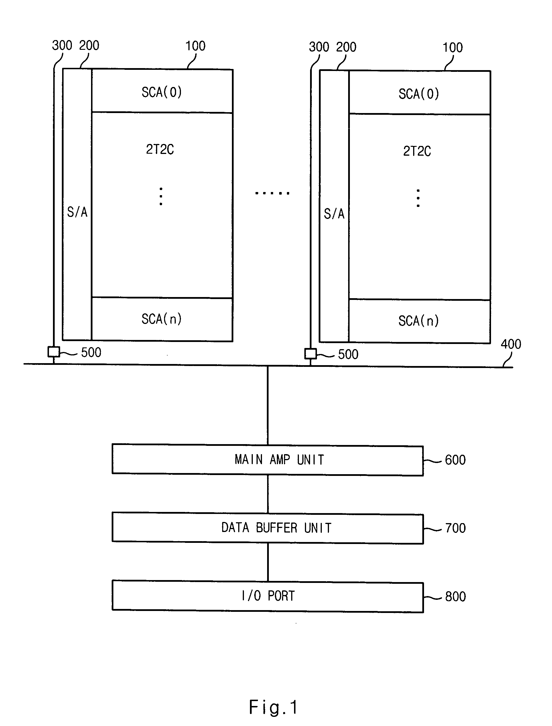
[0022]FIG. 1 is a schematic diagram of a non-volatile ferroelectric memory device according to the present invention.
[0023]In an embodiment, the ferroelectric memory device includes a plurality of cell array blocks 100, a plurality of sense amplifier units 200, a plurality of local data buses 300, a global data bus 400, a plurality of data bus switches 500, a main amplifier 600, and a data bus 700.
[0024]The cell array block 100 consists of a plurality of sub cell arrays SCA(0)-SCA(n) for storing differential data. More specifically, each sub cell array SCA(0)-SCA(n) does not store one data with one unit cell, but stores one data with a plurality of unit cells (e.g., two unit cells in the embodiment) corresponding to a plurality of adjacent main bit lines (e.g., two main bit lines in the embodiment). Moreover, each cell array block 100 has a hierarchical bit line architecture including a plurality of main bit lines and a plurality of main bit lines. In the hierarchical architecture, ...
second embodiment
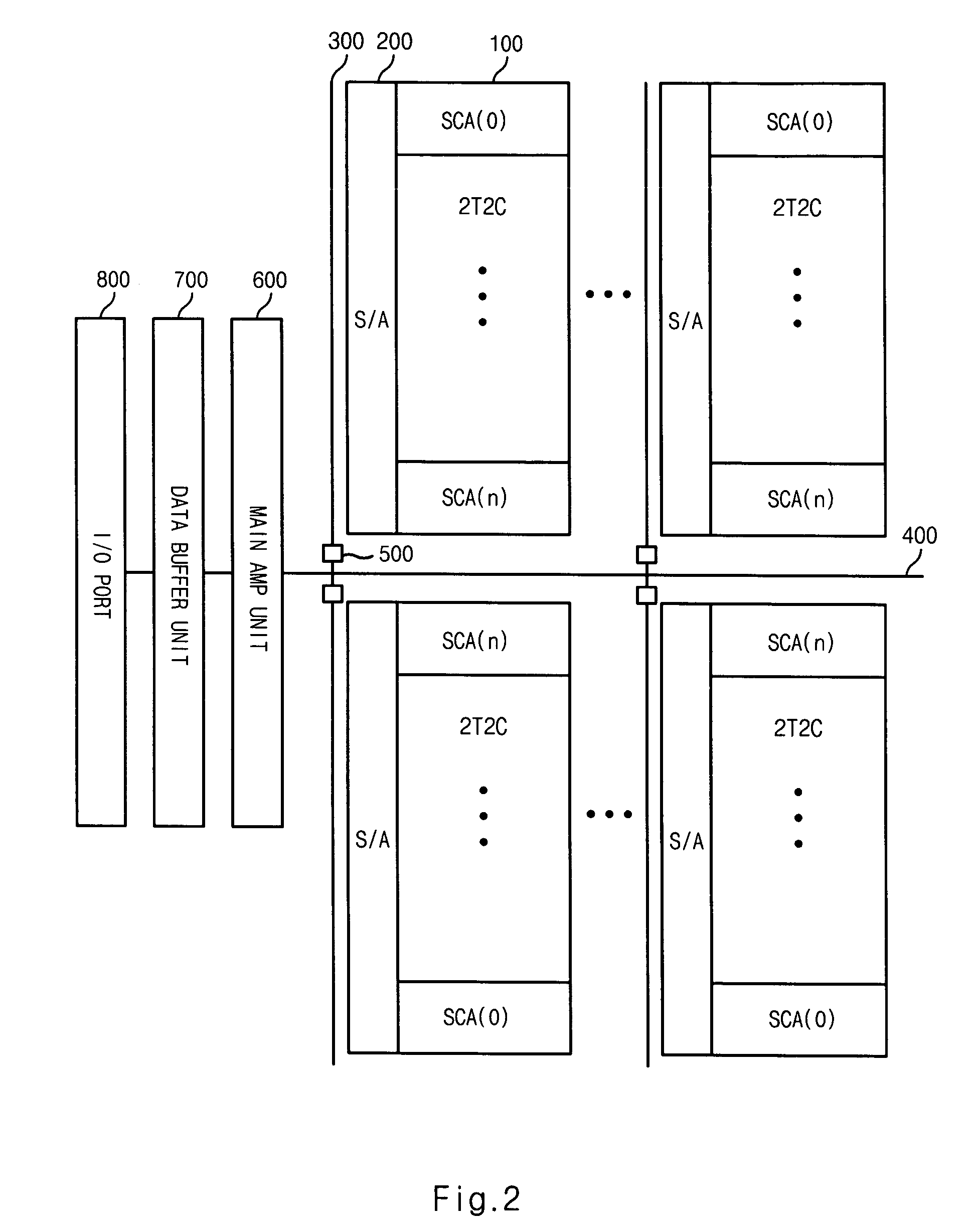
[0030]FIG. 2 is a schematic block diagram of a non-volatile ferroelectric memory device according the present invention.
[0031]In this embodiment shown in FIG. 2, the cell array blocks 100 are divided into two groups (upper cell array blocks and lower cell array blocks) to be vertically symmetric by the global data bus 400. And, in each cell array block 100, the sense amplifier unit 200 corresponds one-by-one the local data bus 300 as shown in FIG. 1.
[0032]The upper and lower local data buses 300 share the global data bus 400 depending on the on / off operation of the data bus switch 500.
[0033]The structure and operation of the other elements are the same as those in FIG. 1.
[0034]FIG. 3 is a circuit diagram illustrating a multi-bit line architecture of sub cell arrays SCA(0)-SCA(n) shown in FIG. 1 and FIG. 2.
[0035]One main bit line MBL is shared by the sub cell arrays SCA(0)-SCA(n), and sub bit lines are respectively provided to the sub cell arrays SCA(0)-SCA(n) to share one main bit l...
PUM
 Abstract
Description
Claims
Application Information


