Yield analysis method

a technology of yield analysis and yield, applied in the field of yield analysis, can solve problems such as loss of yield, systematic failure caused by misprocessing, and loss of wholesale die yield near the edg

Inactive Publication Date: 2008-06-10
TAIWAN SEMICON MFG CO LTD
View PDF2 Cites 6 Cited by
  • Summary
  • Abstract
  • Description
  • Claims
  • Application Information

AI Technical Summary

Benefits of technology

[0012]Accordingly, an object of the invention is to provide a yield analysis method. The yield analysis method is capable of calculating respective systematic limited yield and random defect limited yield from a known overall yield data and of decomposing the systematic limited yield into localized-failure-excluded and repeated-failure-excluded yield data.

Problems solved by technology

These yield losses may be the result of random defects or systematic failures.
Some systematic failures caused by mis-processing escape inline optical inspections in the fabrication process as well as during parametric testing.
The thickness of films deposited on the wafer is often well-controlled across the central portion of the wafer but poorly near the edge, resulting in wholesale die yield loss near the edge.
Hence, systematic failures such as edge losses and random defects are factors in die yield loss.
In practice, however, the defects often occur in clusters or display other systematic patterns.
In general, these spatially clustered defects have assignable causes that can be traced to individual machines or to a series of process steps not meeting specified requirements.
The overall yield is conventionally decomposed into systematic limited yield and defect limited yield.
However, there is no effective way to individually calculate systematic limited yield and defect limited yield from known overall yield data.

Method used


Image

  • Yield analysis method
  • Yield analysis method
  • Yield analysis method

Examples


Embodiment Construction

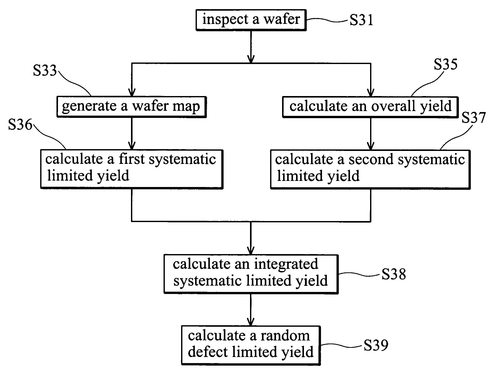
[0033]With reference to the accompanying drawings, embodiments of the present invention are described. In these embodiments, the yield analysis method or system is implemented in wafer fabrication, wherein each processed wafer comprises 460 dies.

[0034]FIG. 3 is a flowchart showing the yield analysis method of the invention. In step S31, a wafer having 460 dies is inspected to obtain wafer defect data containing defect information for every die in the wafer. The wafer defect data is generated by various test and measurement devices such as focused ion beam, electronic microscope, inspector, defect-scanning machine, in-situ particle inspector, and other inspection devices. The wafer defect data shows that among the 460 dies in the wafer, 112 dies are defective and the other 348 dies are not.

[0035]Then a wafer map is generated in step S33 and an overall yield is calculated in step S35 according to the wafer defect data. The overall yield is 75.65%, calculated by dividing the number of ...


PUM


Abstract

A yield analysis method. First, a wafer having multiple dies is inspected to obtain wafer defect data containing defect information for every die in the wafer. Then a wafer map and an overall yield are generated according to the wafer defect data. The wafer map displays defective dies and defect-free dies in the wafer. Then, first and second systematic limited yields are calculated in accordance with the wafer defect data and the wafer map, wherein the first systematic limited yield is calculated excluding defective dies with localized distribution, and the second systematic limited yield is calculated excluding defective dies with repeated distribution. Then a random defect limited yield is determined in accordance with the overall yield, the first systematic limited yield, and the second systematic limited yield.

Description

BACKGROUND OF THE INVENTION[0001]1. Field of the Invention[0002]The present invention relates to yield analysis, and in particular, to a yield analysis method capable of distinguishing random defect yield losses and systematic failure causing yield losses.[0003]2. Description of the Related Art[0004]With multi-billion dollar semiconductor fabrication facilities experiencing increased time-to-market pressures, accurate yield analysis and rapid yield improvement are essential to achieve profitable production of integrated circuits. For maximum competitiveness, cost per die must be minimized while quickly elevating the manufacturing yield to an economically acceptable level.[0005]As shown in FIG. 1, defect inspection data of a wafer is depicted as a wafer map. A wafer 10 has a plurality of arrays of IC devices or chips, wherein each dark color marker 11 represents a failed chip and each blank color marker 13 represents a good chip.[0006]These yield losses may be the result of random de...

Claims


Application Information

Patent Timeline
Patent Type & Authority Patents(United States)
IPC IPC(8): G06F17/18
CPCH01L22/20
Inventor LIN, CHEN-TINGWU, CHIH-HUNGLI, MEI-YEN
Owner TAIWAN SEMICON MFG CO LTD
Why Eureka
Try Eureka