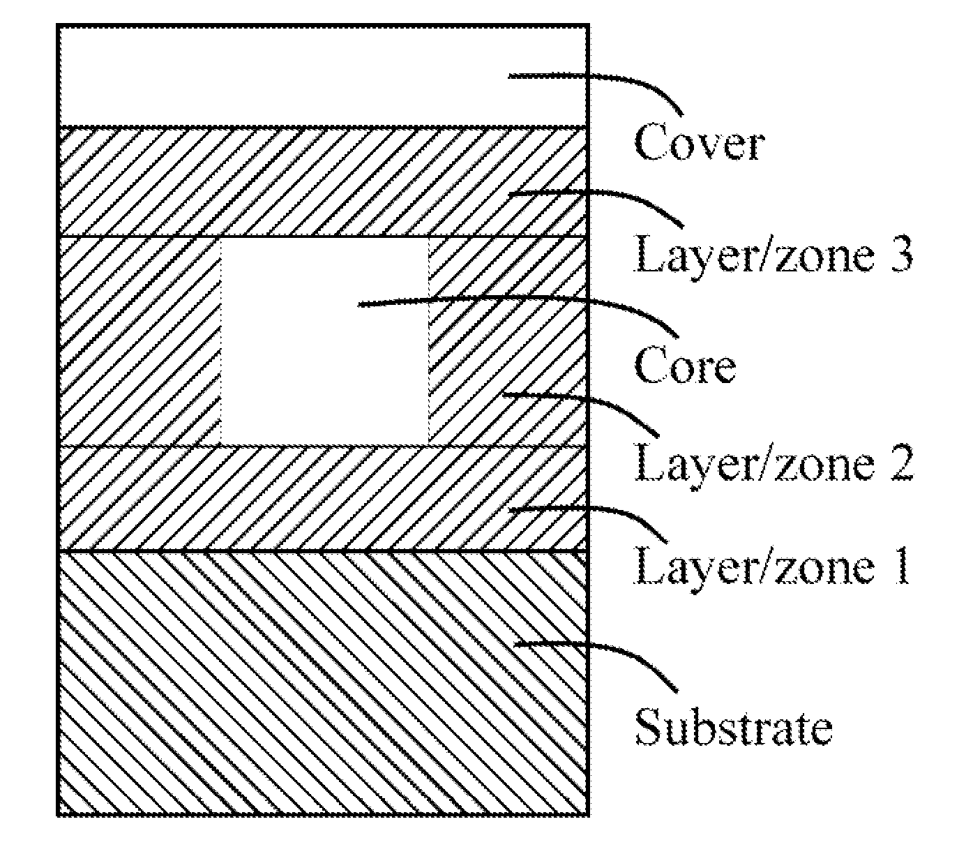
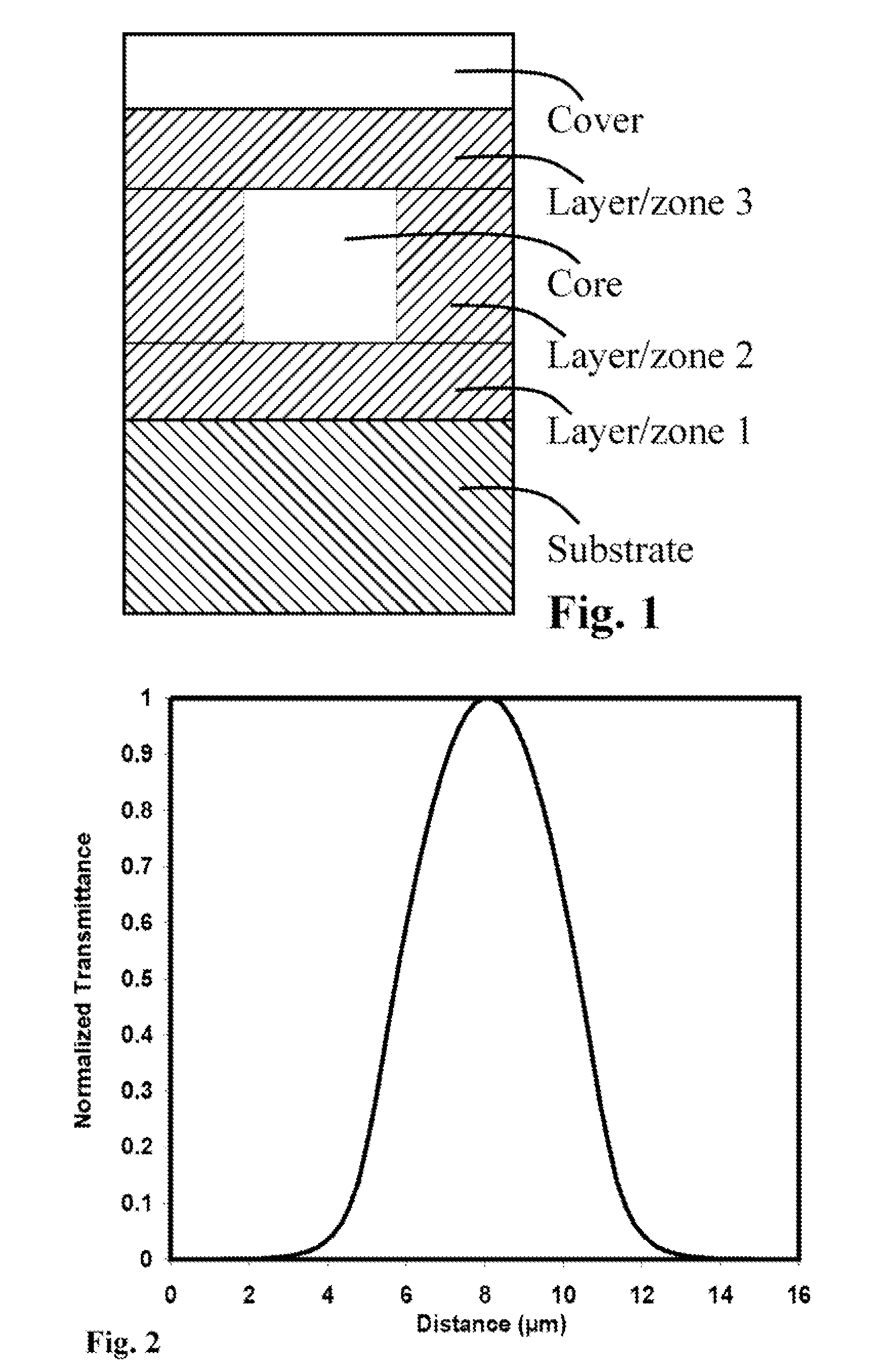
[0015]Here we describe the natural index contrast principle for waveguide formation and fabrication. When two layers of two different materials are brought in contact of each other at an interface, there exists an energy difference similar to the energy levels produced in a semiconductor by dopant atoms. In case of dielectric thin films of two different materials, one laid down or formed on top of another (without any air gap), there will be a difference in refractive index (RI) between the two layers. Light, incident at an appropriate angle on these layers, will bend towards the higher RI material at the interface (the total internal reflection). When a higher RI material is completely enclosed in a lower RI material, incident light will propagate within the enclosed region thus forming a waveguide, similar to a step index optical fiber. The guiding layer is called the core and the surrounding layer is called the cladding. In the NIC principle, refractive index difference between the core and cladding layers are pre-built by materials design. This allows more flexibility to tailor waveguiding requirements for multiple photonic functionalities.
[0017]The present invention discloses an alternative method where built-in refractive index difference of compatible materials is used to form the waveguide core and cladding, thus avoiding direct doping of glasses. This method, called the natural index contrast (NIC) method is an attractive alternative for photonic waveguide design. Here the materials are matched to form the core and the cladding utilizing the built-in index contrast. This eases a big hurdle of controlling the RI via doping methods. The NIC method offers a straightforward solution to produce a step index profile with the possibility to expand to graded index profile as well, while fabrication is significantly simpler than contemporary methods. Since the PICs are based on step index waveguides, NIC method is suitable for a number of PIC based devices. The concept is applicable to any photonic waveguide design where the built-in refractive index contrast is suitable for waveguiding from a chosen set of material. The present invention focuses on waveguides suitable for guiding light in the range of 1060 nm and 1650 nm.
[0019]What distinguishes dendrimers from other materials is the fact that it offers properties similar to dielectric materials in a polymeric form. Dendrimers are a novel class of three-dimensional nanoscale, core-shell molecules that can be precisely synthesized for a wide range of applications. Building on a central core molecule, dendrimer molecules are formed by the step-wise, sequential addition of concentric shells consisting of branched molecules and connector groups. Each branched shell is referred to as a generation. Up to ten generations can be incorporated into a single dendrimer molecule, thus allowing a wide range control of the size and number of functional groups of each molecule. Some important properties of this class of polymers can be found at the DNT web at http: / / dnanotech.com / properties.html.
[0028]At the second phase of integration, appropriate on-chip gain elements (e.g., Er3+ doped waveguide amplifier) can be combined with these chips to produce the above mentioned PICs with low-loss and / or with a gain. This is important, because, optical transmission systems require frequent signal amplification and regeneration (also called repeater) that is expensive and adds complexity to system design. Ability to build systems with extremely low-loss and / or gain will simplify system design significantly. It will also eliminate the frequent need of signal regeneration, thus enabling significant cost savings and ease of deployment of fiberoptic systems.
[0031]The objective of a chip-scale PIC is to produce a very concise device with multiple functionalities on a single substrate. Two different schemes are usually considered: (i) system-on-chip, and (ii) chip-scale packaging; both of these schemes actually complement each other. The triple-phase integration scheme, as described above, allows a PIC (e.g., a RAWG) to be further integrated over several phases to produce denser functionality on the same substrate. For instance, a RAWG monolithically attached with amplifying waveguide blocks allows controlling the loss factor. Further, lasers and modulators can be added to the RAWG to produce multichannel transmitters. One can then add detectors to add more functionality enabling transceivers, transponders, and switching on a chip as well. Finally, combined with CMOS processes, these PICs can be used to build self containing optical communication router. However, here we emphasize on monolithic integration, as opposed to hybrid integration where different elements are packaged together on a single substrate or in a single box.

