
Method for manufacturing printing plate

a printing plate and liquid crystal technology, applied in the field of liquid crystal display (lcd) devices, can solve the problems of difficult to realize high resolution, low yield of printing methods, and broken glass substrates, and achieve precise and fine patterns

Inactive Publication Date: 2008-06-24
LG DISPLAY CO LTD
View PDF1 Cites 5 Cited by
  • Summary
  • Abstract
  • Description
  • Claims
  • Application Information

AI Technical Summary

Benefits of technology

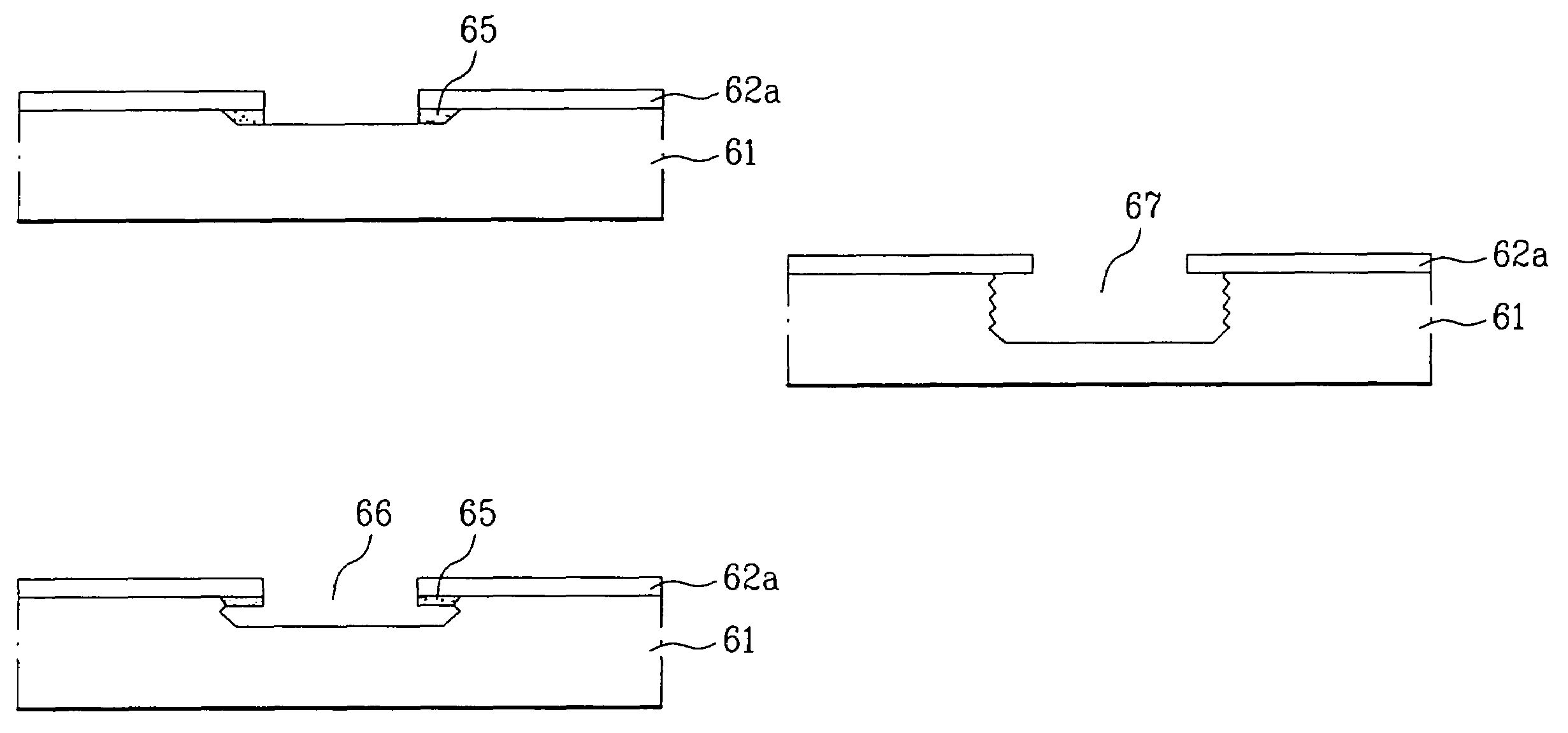
The invention is a method for manufacturing a printing plate that can create precise and fine patterns by minimizing variations in etching critical dimension. The method involves forming a hard mask with an opening over an insulating substrate, creating a first trench with a first depth in the substrate, coating a photoresist over the substrate and patterning it using the hard mask, creating a second trench with a second depth in the substrate, coating a second photoresist over the substrate and patterning it using the hard mask, creating a third trench with a third depth in the substrate, and removing the hard mask. The method can create a printing plate that can produce more precise and fine patterns.

Problems solved by technology

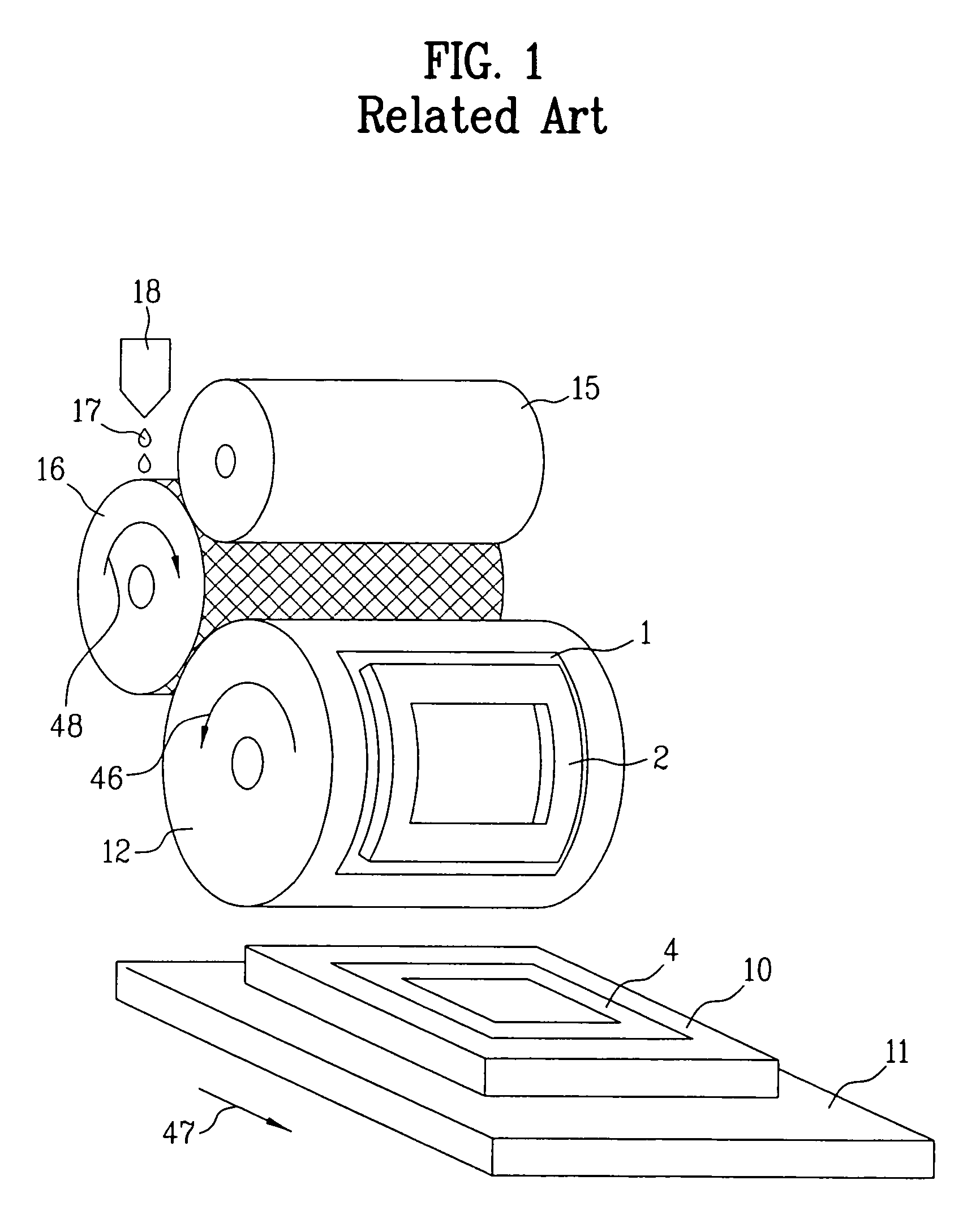
Accordingly, the printing method has low yield.
In addition, since the glass substrate is deformed, it is difficult to realize high resolution.
Second, the sandblasting method is used to produce a fine wall of a large-sized panel.
However, the glass substrate may be broken due to physical impact during firing.
Also, the process of sandblasting is complicated, whereby the manufacturing cost increases.
Further, an environmental pollution may be generated due to dust.
As a result, it is difficult to manufacture a precise printing plate.

Method used


Image

  • Method for manufacturing printing plate
  • Method for manufacturing printing plate
  • Method for manufacturing printing plate

Examples


Embodiment Construction

[0039]Additional advantages, objects, and features of the invention will be set forth in part in the description which follows and in part will become apparent to those having ordinary skill in the art upon examination of the following or may be learned from practice of the invention. The objectives and other advantages of the invention may be realized and attained by the structure particularly pointed out in the written description and claims hereof as well as the appended drawings.

[0040]Reference will now be made in detail to the preferred embodiments of the invention, examples of which are illustrated in the accompanying drawings. Wherever possible, the same reference numbers will be used throughout the drawings to refer to the same or like parts.

[0041]FIGS. 3A to 3H show cross sectional views illustrating a method for manufacturing a printing plate according to the invention.

[0042]As shown in FIG. 3A, a metal layer 62 for a hard mask is deposited on an insulating glass substrate...


PUM

PropertyMeasurementUnit
heightaaaaaaaaaa
heightaaaaaaaaaa
depthaaaaaaaaaa

Abstract

A method for manufacturing a printing plate is realizes a precise and fine pattern by minimizing a variation of etching critical dimension. The method includes forming a hard mask having an opening on an insulating substrate; forming a first trench having a first depth in the insulating substrate using the hard mask; coating, patterning and developing a first photoresist over an entire surface of the insulating substrate including the hard mask; and forming at least a second trench having a second depth in the insulating substrate using the hard mask, wherein the second depth is deeper than the first depth.

Description

[0001]This application claims the priority under 35 U.S.C. §119 of the Korean Patent Application No. 10-2005-58303, filed on Jun. 30, 2005, which is hereby incorporated by reference as if fully set forth herein.BACKGROUND OF THE INVENTION[0002]1. Field of the Invention[0003]The invention relates to a method for manufacturing a liquid crystal display (LCD) device, and more particularly, to a method for manufacturing a printing plate to realize a fine pattern.[0004]2. Description of the Related Art[0005]Various displays that can substitute for a cathode ray tube (CRT) have recently been developed, which have various advantages of portability, light weight, thin profile, small size, good picture quality, etc.[0006]In general, an LCD device is includes a thin film transistor (TFT) array substrate, a color filter substrate, and a liquid crystal layer formed between the TFT array substrate and the color filter substrate. On the TFT array substrate, multiple gate lines are formed in perpen...

Claims


Application Information

Patent Timeline
Patent Type & Authority Patents(United States)
IPC IPC(8): B44C1/22
CPCG03F7/0035G02F1/1339G03F7/0007G03F7/40G02F1/136
Inventor YOO, SOON SUNGKWON, OH NAMCHO, HEUNG LYULLEE, JUNG JAENAM, SEUNG HEE
Owner LG DISPLAY CO LTD
Learn More