LDMOS transistor device employing spacer structure gates

a transistor device and spacer structure technology, applied in the field of integrated circuit technology, can solve the problems of unconsidered full improvement potential, unnecessary high input capacitance, and unnecessary low speed, and achieve the effects of reducing input capacitance, increasing the speed of the ldmos transistor device, and significantly reducing the gate length

Inactive Publication Date: 2008-06-24
INFINEON TECH AG
View PDF15 Cites 43 Cited by
  • Summary
  • Abstract
  • Description
  • Claims
  • Application Information

AI Technical Summary

Benefits of technology

[0014]By providing an LDMOS transistor device in an integrated circuit, particularly an integrated circuit for radio frequency applications, comprising a novel split gate structure the gate length is considerably decreased, thereby reducing the input capacitance and increasing the speed of the LDMOS transistor device.

Problems solved by technology

Some prior art solutions do not take the full improvement potential into account.
For instance, some of the prior art LDMOS transistors of the above-mentioned kind have still an unnecessary high input capacitance and thereby an unnecessary low speed.

Method used


Image

  • LDMOS transistor device employing spacer structure gates
  • LDMOS transistor device employing spacer structure gates
  • LDMOS transistor device employing spacer structure gates

Examples


Embodiment Construction

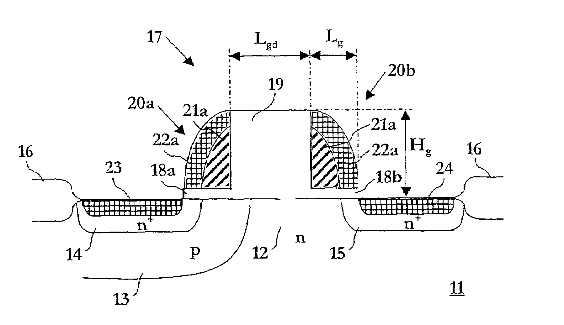
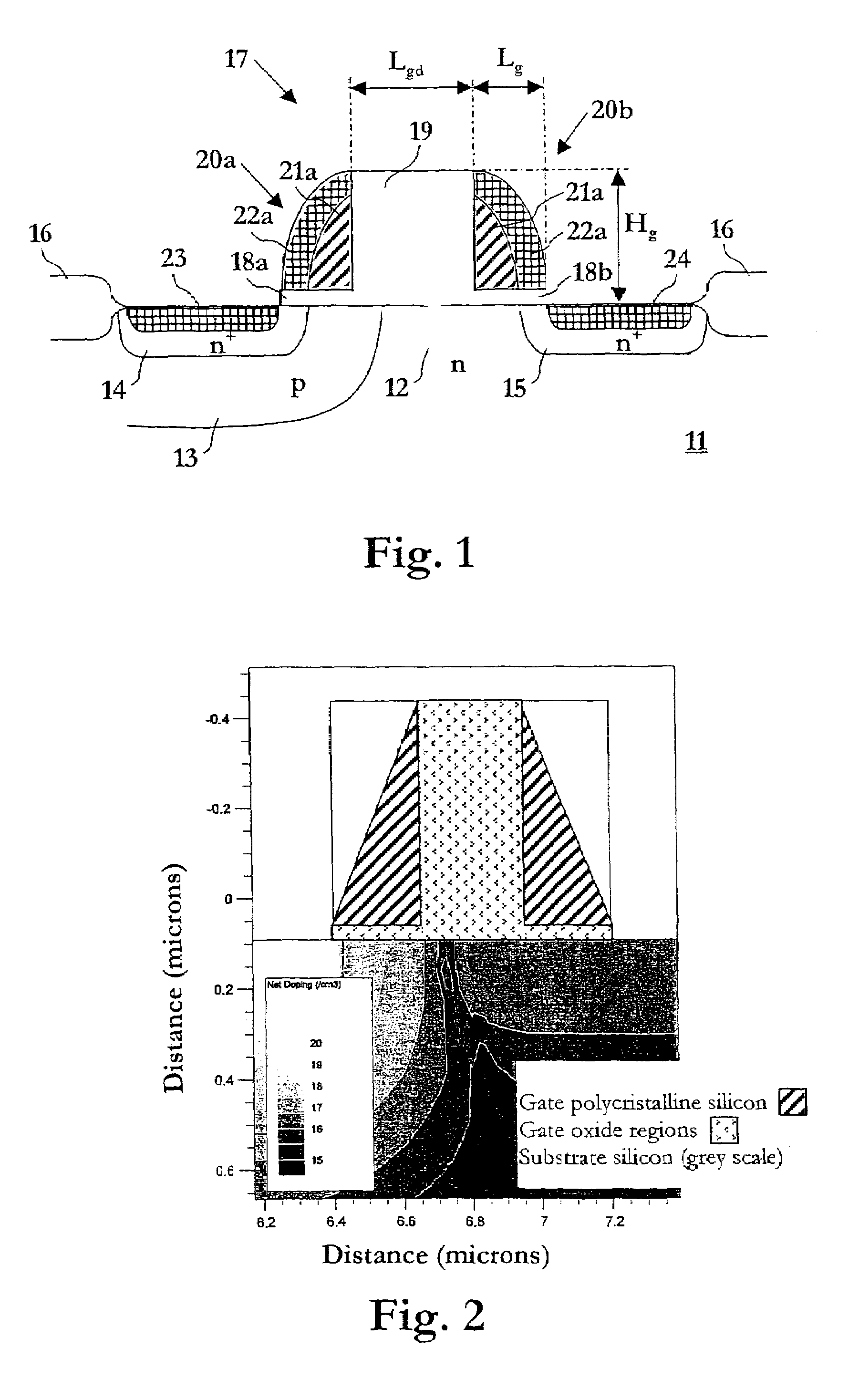
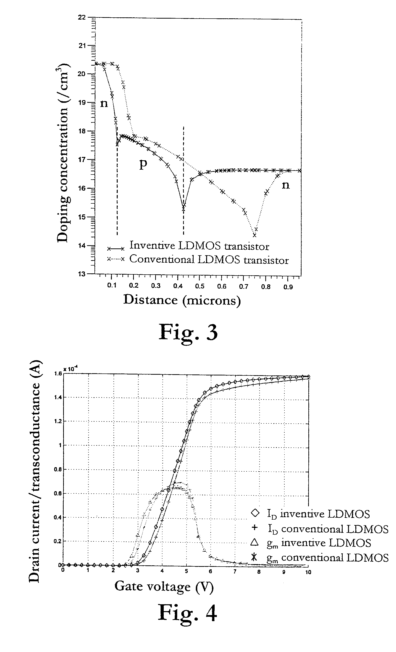
[0025]A silicon LDMOS transistor according to a first preferred embodiment of the present invention is shown in FIG. 1 in an enlarged cross-sectional view. The LDMOS transistor, which is particularly adapted for high power radio frequency applications, comprises a semiconductor substrate 11, in which n31-type doped drain drift 12, p-type doped channel pocket 13, n+-type doped source 14, and n+-type doped drain 15 regions are formed. The doped regions 12-15 in the substrate 11 are laterally surrounded by field oxide 16 or other kind of insulation areas, such as e.g. shallow trench isolation (STI) regions.

[0026]An inventive LDMOS gate structure 17 is arranged on top of the substrate 11. The gate structure 17 includes a centrally located split gate-dividing separator 19 of an electrically insulating material and a first 18a and a second 18b gate insulation layer region on a respective side of the split gate-dividing separator 19. The split gate-dividing separator 19 has a length Lgd an...


PUM


Abstract

An integrated LDMOS transistor comprises a semiconductor substrate (11), an LDMOS gate region (17), LDMOS source (14) and drain (15) regions, and a channel region (13) arranged beneath the LDMOS gate region, where the channel region interconnects the LDMOS source and drain regions. The LDMOS gate region comprises first (18a) and second (18b) gate insulation layer regions, a centrally located gate-dividing insulation region (19) provided between the first and second gate insulation layer regions, and first (20a) and second (20b) individual gate conducting layer regions, each being provided on top of a respective one of the first and second gate insulation layer regions, and each being an etched outside spacer region at the centrally located insulation layer region.

Description

PRIORITY[0001]This application claims priority to Swedish application No. 0303106-9 filed Nov. 21, 2003.TECHNICAL FIELD OF THE INVENTION[0002]The present invention generally relates to the field of integrated circuit technology, and more specifically the invention relates to an LDMOS (lateral double diffused MOS) transistor device, to an integrated circuit including the LDMOS transistor device, and to a fabrication method of the integrated circuit with the LDMOS transistor device, respectively.DESCRIPTION OF RELATED ART AND BACKGROUND OF THE INVENTION[0003]The speed of an LDMOS transistor is determined by the transconductance gm and the input capacitance Cin, and more specifically, the speed is proportional to gm / Cin. By reducing the capacitance without changing the transconductance, the speed is increased with no additional drawbacks assuming that the process lithography is maintained unaffected.[0004]An improved performance using a scaled down device with a channel length shorter ...

Claims


Application Information

Patent Timeline
Patent Type & Authority Patents(United States)
IPC IPC(8): H01L29/76H01L21/28H01L21/336H01L29/423H01L29/45H01L29/49H01L29/78
CPCH01L21/2815H01L29/42376H01L29/402H01L29/66681H01L29/7816H01L29/456H01L29/4933H01L29/7831
Inventor ARNBORG, TORKELSMITH, ULF
Owner INFINEON TECH AG
Why Eureka
Try Eureka