Clock distribution network designers face the problem of designing clock
distribution networks that distribute clock signals throughout an integrated circuit device or system with a minimal level of
clock skew.
The principle cause of
clock skew in clock distribution networks is the variation in the routing impedance of various branches of the clock distribution network.
Consequently, clock skew may arise within an individual integrated circuit die even where an equal length clock distribution network such as an H-Tree is employed.
If skew increases beyond a certain time period, setup and
hold time problems may be unavoidable.
It should be appreciated, however, that as VLSI clock frequencies increase beyond 1 GHz, the distribution network design constraints presented by clock skew become even more challenging.
However, as circuit components (flip
flops etc.) increase it becomes more difficult at the
block level for the auto routing tool to provide a buffer tree that balances clock skew.
Building
chip level buffer trees using auto routing tools become more difficult as the number of blocks in a design increase.
The process is further complicated by the need to have provided a timing number for each of the blocks in a design.
As the design size increases to levels that encompass millions of gates, the clock skew exhibited by a network may increase prohibitively.
Within a single block clock skew may be manageable, but may become increasingly difficult as the designer progresses to the
chip level.
Moreover, as systems become more complicated utilizing increasingly faster operating frequencies, it becomes extremely difficult to resolve clock skew problems at the
chip level (e.g., using the balanced buffer tree approach) without substantial manual input.
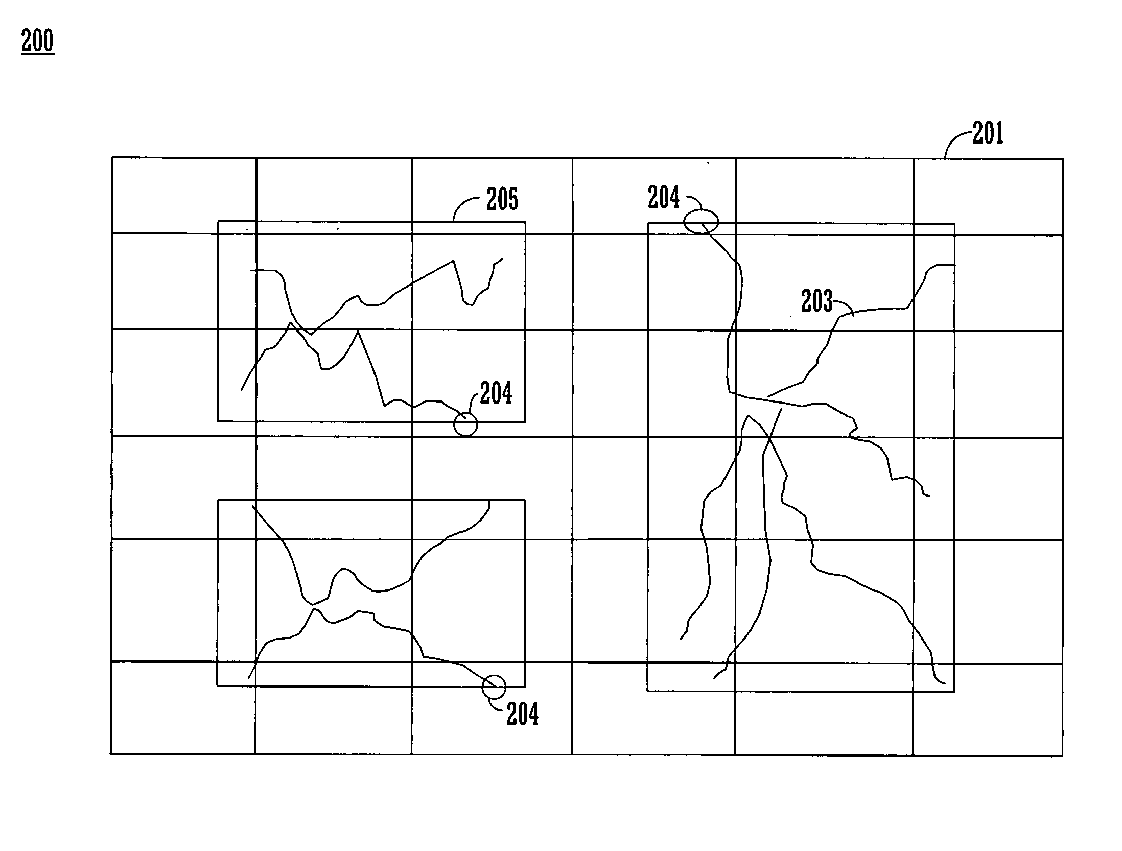
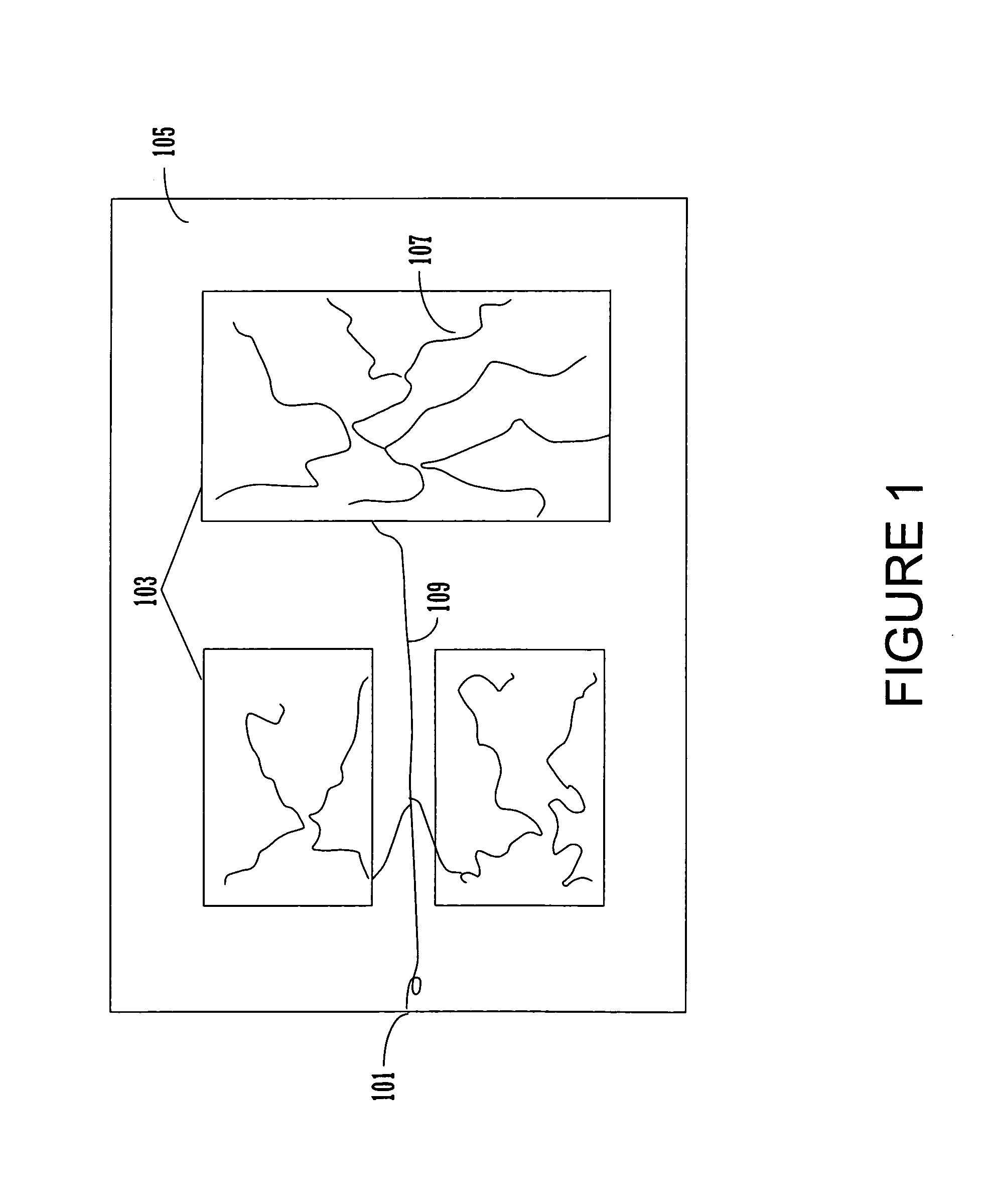
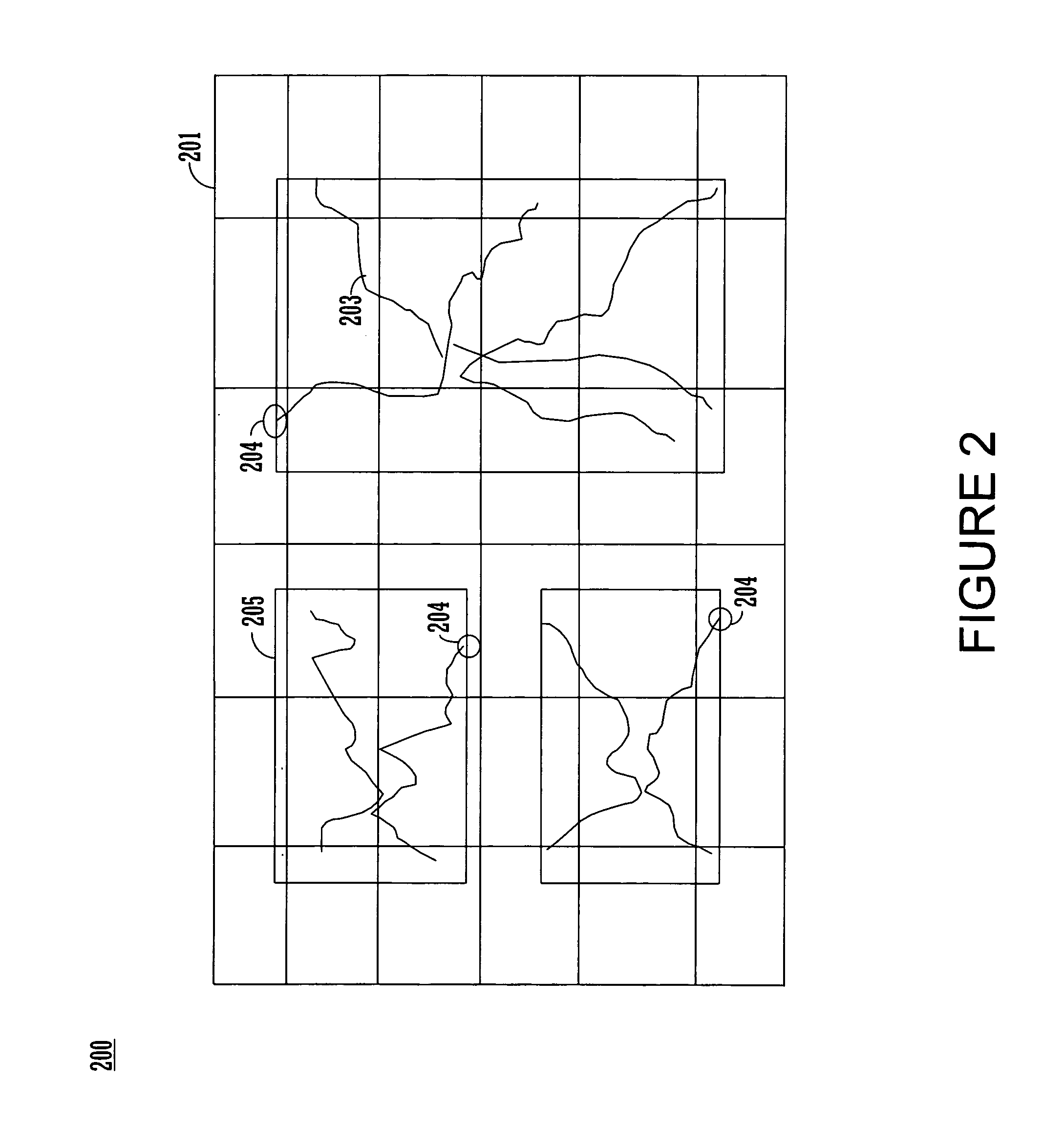
A drawback of this approach includes the difficulty in achieving a balanced skew across the blocks of the integrated circuit 105 at the chip level.
This is a consequence of the difficulty posed in predicting the routing characteristics of the routes traversed by clock signals (input at clock pin 101) that are transmitted through the clock distribution network.
However, because the
delay of each component in the system must be managed, systems that employ millions of components require extensive manual
layout work.
Additional drawbacks of this scheme include its lack of hierarchical intricacy, its routing track intensiveness, the long turn around times manifest in its production, and the lack of tool support available for creation and analysis purposes.
It should be appreciated that, skew prediction at the chip level is very difficult with either of these schemes, and accommodating multiple clock domains may present significant challenges.

