Asymmetrically stressed CMOS FinFET

a technology of cmos and finfet, which is applied in the field of field effect transistors, can solve the problems of pfets and nfets being supplied with opposite stress materials, affecting the quality of pfets and nfets, and being generally costly and complicated to fabrica

Active Publication Date: 2008-07-15
GLOBALFOUNDRIES U S INC
View PDF11 Cites 6 Cited by
  • Summary
  • Abstract
  • Description
  • Claims
  • Application Information

AI Technical Summary

Problems solved by technology

Thus, there is the complication of the need to supply oppositely stressed materials for pFETs and nFETs if the switching speed is to be optimal for both simultaneously.
Conventional CMOS devices typically involve either favorably straining only pFETs or nFETs while relieving the strain on the opposite type, or be depositing separate straining films for each type of FET, which is generally costly and complicated to fabricate.

Method used


Image

  • Asymmetrically stressed CMOS FinFET
  • Asymmetrically stressed CMOS FinFET
  • Asymmetrically stressed CMOS FinFET

Examples


Embodiment Construction

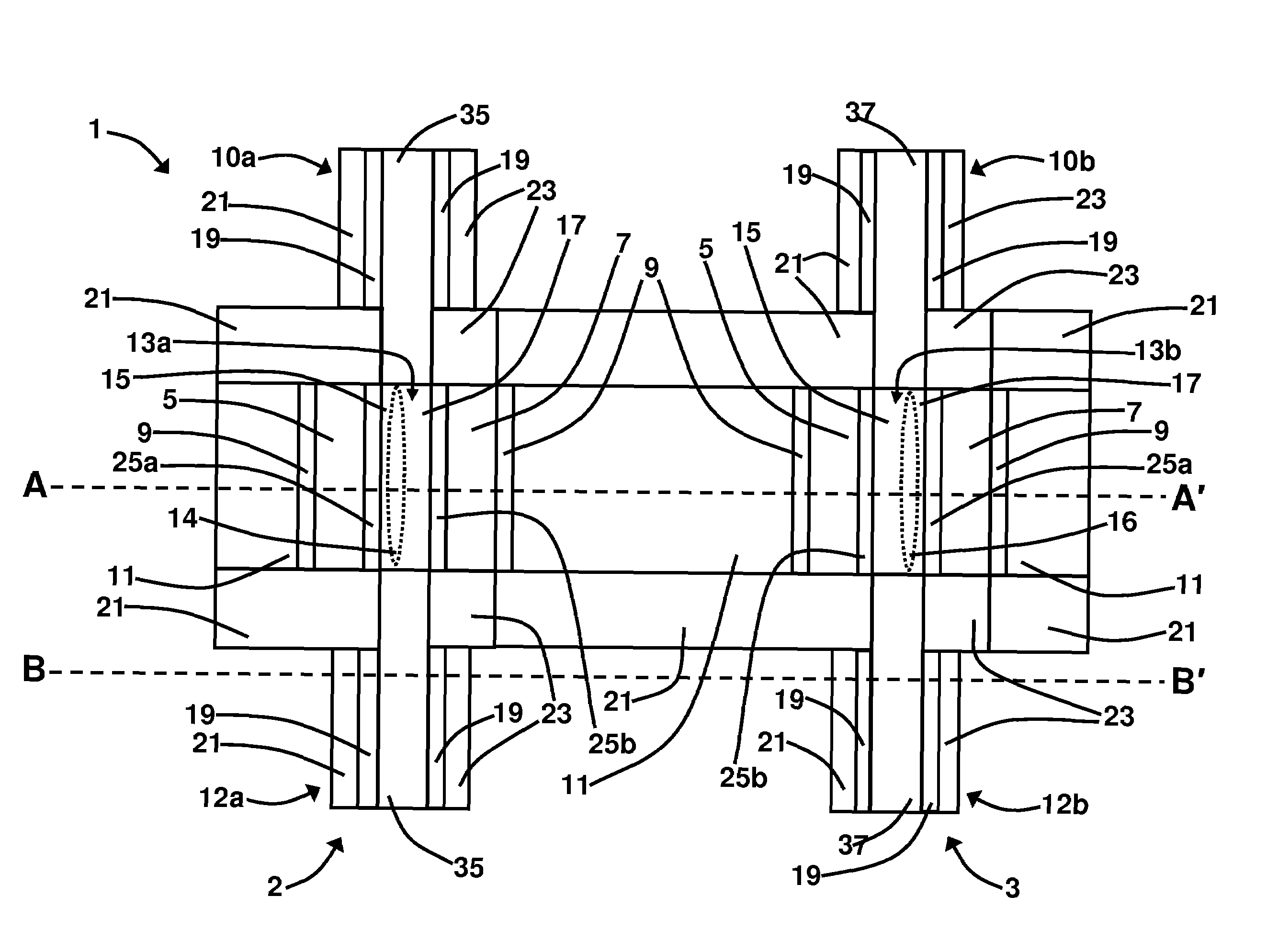
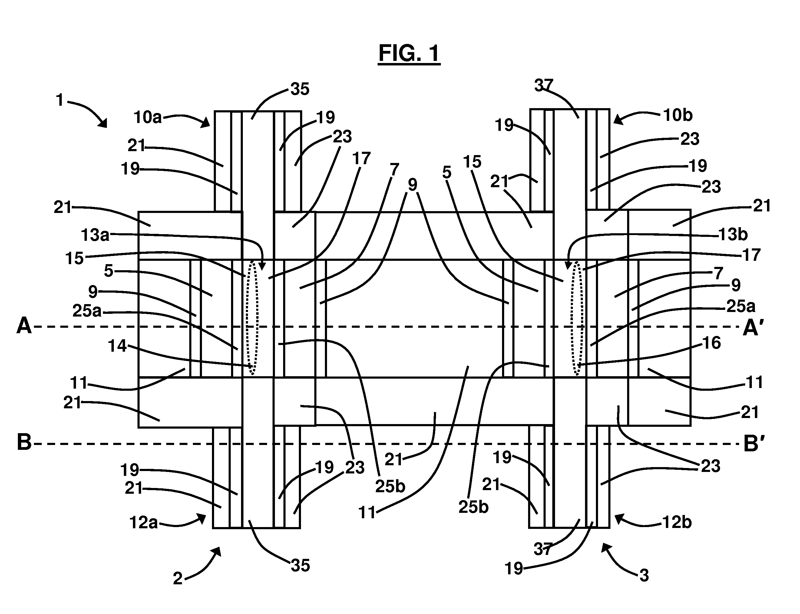
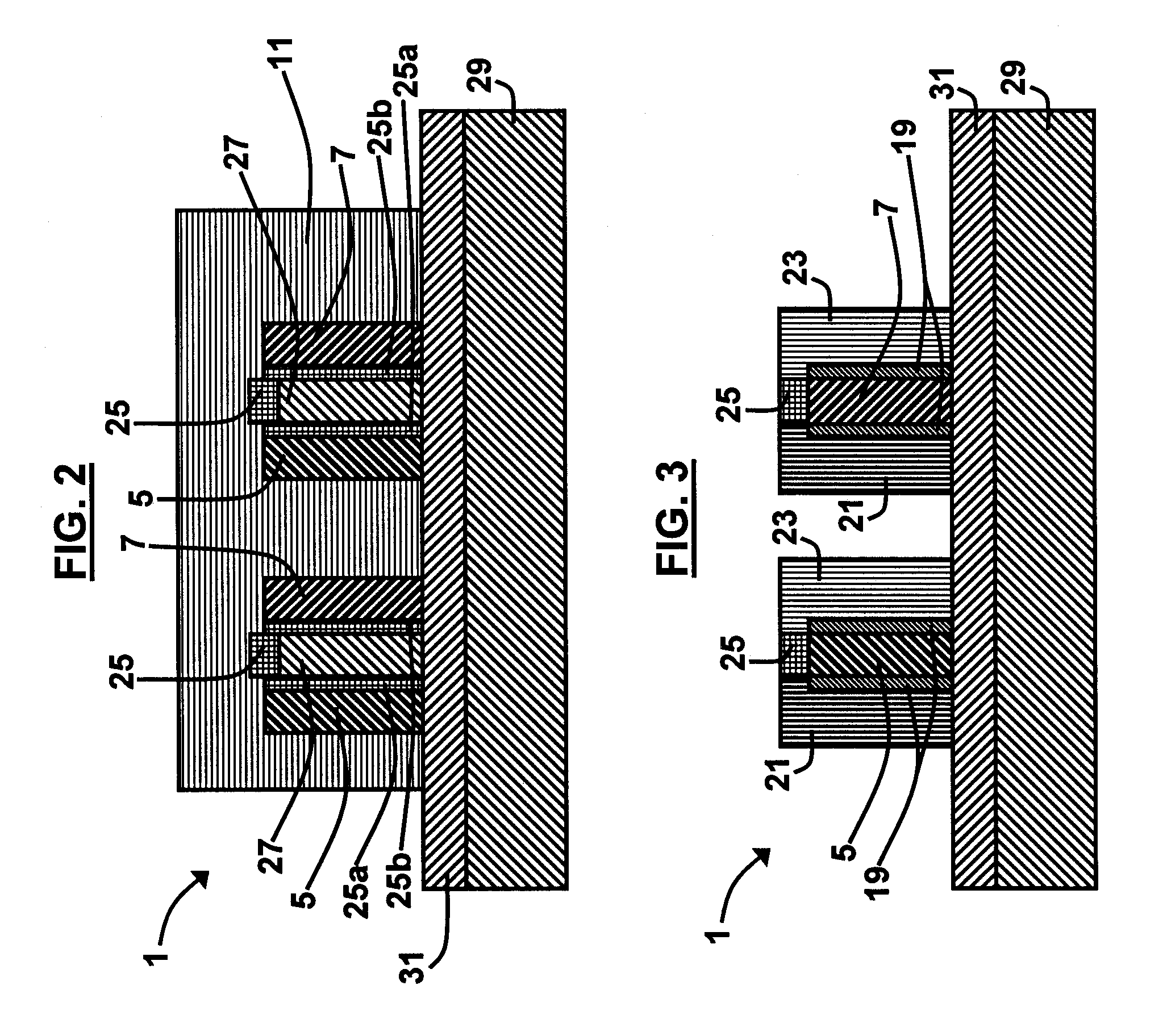
[0016]The embodiments of the invention and the various features and advantageous details thereof are explained more fully with reference to the non-limiting embodiments that are illustrated in the accompanying drawings and detailed in the following description. It should be noted that the features illustrated in the drawings are not necessarily drawn to scale. Descriptions of well-known components and processing techniques are omitted so as to not unnecessarily obscure the embodiments of the invention. The examples used herein are intended merely to facilitate an understanding of ways in which the embodiments of the invention may be practiced and to further enable those of skill in the art to practice the embodiments of the invention. Accordingly, the examples should not be construed as limiting the scope of the embodiments of the invention.

[0017]As mentioned, there is the complication of the need to supply oppositely stressed materials for pFETs and nFETs if switching speed is to b...


PUM


Abstract

A CMOS device comprising a FinFET comprises at least one fin structure comprising a source region; a drain region; and a channel region comprising silicon separating the source region from the drain region. The FinFET further comprises a gate region comprising a N+ polysilicon layer on one side of the channel region and a P+ polysilicon layer on an opposite side of the channel region, thereby, partitioning the fin structure into a first side and a second side, respectively. The channel region is in mechanical tension on the first side and in mechanical compression on the second side. The FinFET may comprise any of a nFET and a pFET, wherein the nFET comprises a N-channel inversion region in the first side, and wherein the pFET comprises a P-channel inversion region in the second side. The CMOS device may further comprise a tensile film and a relaxed film on opposite sides of the fin structure adjacent to the source and drain regions, and an oxide cap layer over the fin structure.

Description

BACKGROUND[0001]1. Field of the Invention[0002]The embodiments of the invention generally relate to complementary metal oxide semiconductor (CMOS) devices, and, more particularly, to a field effect transistor (FET) used in a CMOS device.[0003]2. Description of the Related Art[0004]In FET devices, hole mobility is augmented when the channel is under compression in a direction parallel to the current. Electron mobility is augmented when the channel is under tension in a direction parallel to the current. Thus, there is the complication of the need to supply oppositely stressed materials for pFETs and nFETs if the switching speed is to be optimal for both simultaneously. Conventional CMOS devices typically involve either favorably straining only pFETs or nFETs while relieving the strain on the opposite type, or be depositing separate straining films for each type of FET, which is generally costly and complicated to fabricate. Therefore, there remains a need for a novel CMOS device that...

Claims


Application Information

Patent Timeline
Patent Type & Authority Patents(United States)
IPC IPC(8): H01L23/58
CPCH01L21/845H01L27/1211H01L29/785H01L29/4908H01L29/66795H01L29/7843H01L29/42384H01L21/823807H01L29/7856
Inventor ANDERSON, BRENT A.NOWAK, EDWARD J.
Owner GLOBALFOUNDRIES U S INC
Why Eureka
Try Eureka