FinFET SRAM cell with chevron FinFET logic

a technology of finfet and logic, applied in the field of static random access memory (sram) cells, can solve the problems of sram design that could lose the density advantage of finfet technology, which uses various crystal planes, and achieve the effect of reducing the cost of sram design

Inactive Publication Date: 2005-03-15
IBM CORP
View PDF8 Cites 217 Cited by
  • Summary
  • Abstract
  • Description
  • Claims
  • Application Information

AI Technical Summary

Benefits of technology

[0006]A first aspect of the present invention is an electronic device comprising: a semiconductor device comprising: a pass gate transistor including a first fin body and a first gate, the first fin body having opposing sidewalls, each sidewall aligned in a first direction having a first majority carrier mobility, the first gate adjacent to both sidewalls of the first fin body; a pull down latch transistor including a second fin body and a second gate, the second fin body having opposing sidewalls, each sidewall aligned in a second direction having a second majority carrier mobility, the second gate adjacent to both sidewalls of the second fin body; a pull up latch transistor including a third fin body and a third gate, the third fin body having opposing sidewalls, each sidewall aligned in a third direction having a third majority carrier mobility, the third gate adjacent to both sidewalls of the third fin body; wherein all of the first, second and third directions are not the same direction; and one or more CMOS chevron logic circuits, crystal planes of bodies of transistors of the CMOS chevron logic circuits and crystal planes or the first, second and third fin bodies co-aligned.
[0007]A second aspect of the present invention is a method of fabricating a semiconductor device comprising: forming a first fin body of a pass gate transistor from a crystal layer, the first fin body having opposing sidewalls, each sidewall aligned in a first direction having a first majority carrier mobility; forming a second fin body of a pull down latch transistor from the crystal layer, the second fin body having opposing sidewalls, each sidewall aligned in a second direction having a second majority carrier mobility; forming a third fin body or a pull up latch transistor from the crystal layer the third fin body having opposing sidewalls, each sidewall aligned

Problems solved by technology

However, much of the density advantage of FinFET technology, which us

Method used


Image

  • FinFET SRAM cell with chevron FinFET logic
  • FinFET SRAM cell with chevron FinFET logic
  • FinFET SRAM cell with chevron FinFET logic

Examples


second embodiment

ating the layout of an SRAM cell according to the present invention

[0018]FIG. 11 is a diagram illustrating the layout of an SRAM cell according to a first alternative of a third embodiment of the present invention; and

[0019]FIG. 12 is a diagram illustrating the layout of an SRAM cell according to a second alternative of a third embodiment of the present invention.

DETAILED DESCRIPTION

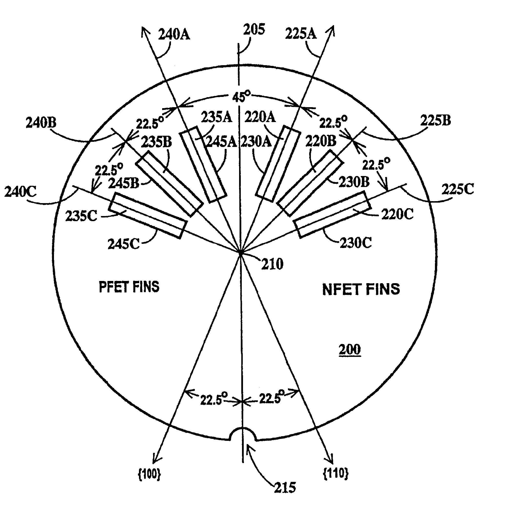
[0020]In crystalline solids, the atoms, which make up the solid, are spatially arranged in a periodic fashion called a lattice. A crystal lattice always contains a volume, which is representative of the entire lattice and is regularly repeated throughout the crystal. In describing crystalline semiconductor materials in the present disclosure, the following conventions will be used.

[0021]The directions in a lattice are expressed as a set of three integers with the same relationship as the components of a vector in that direction. For example, in cubic lattices, such as silicon, that has a diamond crystal ...


PUM


Abstract

An electronic device, and SRAM and a method of forming the electronic device and SRAM. The semiconductor device including: a pass gate transistor having a fin body having opposing sidewalls aligned in a first direction and having a first majority carrier mobility and a gate adjacent to both sidewalls of the fin body; a pull down latch transistor having a fin body having opposing sidewalls aligned in a second direction and having a second majority carrier mobility and a gate adjacent to both sidewalls of thc fin body; a pull up latch transistor having a fin body having opposing sidewalls aligned in a third direction and having a third majority carrier mobility and a gate adjacent to both sidewalls of the fin body; and CMOS chevron logic circuits, wherein crystal planes of each fin body and of CMOS transistor of the chevron logic are co-aligned.

Description

BACKGROUND OF INVENTION[0002]1. Field of the Invention[0003]The present invention relates to the field of semiconductor devices; more specifically, it relates to a static random access memory (SRAM) cell using fin field effect transistor (FinFET) technology.[0004]2. Background of the Invention[0005]The need for increased device density in CMOS integrated circuits has led to the use of FINFET CMOS logic circuits. In a FinFET vertical “fins” of crystalline silicon are used to form the body of each transistor and gates are formed on each side of the body. When gates are formed on both sides of the body, the transistor is generally referred to as a double gate FinFET. An advantage of FinFET transistors is that the “fin” can be formed so that the channel region of each transistor is aligned relative to the crystal planes of the silicon allowing control of the majority carrier mobility of both PFETs and NFETs independently which is not possible in standard (planar) CMOS technology. Howeve...

Claims


Application Information

Patent Timeline
IPC IPC(8): H01L21/70H01L29/786H01L21/02H01L29/66H01L27/12H01L21/336H01L27/11H01L21/8244H01L21/84H01L27/02H01L29/04
CPCH01L21/845H01L27/0207H01L27/11H01L27/1104H01L29/045H01L29/66795H01L29/785H01L27/1211Y10S257/903H10B10/00H10B10/12
Inventor ANDERSON, BRENT A.BRYANT, ANDRESNOWAK, EDWARD J.
Owner IBM CORP
Why Eureka
Try Eureka